AIWA CDC-Z107 Service Manual - Page 30
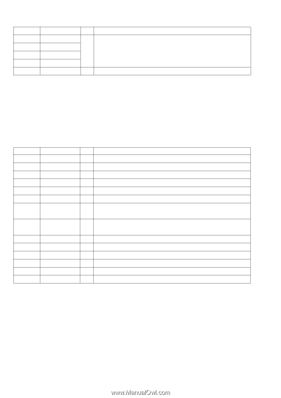
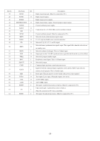
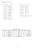
Pin No., Pin Name, Description, IC, LC75853NW
 |
View all AIWA CDC-Z107 manuals
Add to My Manuals
Save this manual to your list of manuals |
Page 30 highlights
Pin No. 40 41 42 43 44 Pin Name TP(R) TUN(R) CD(R) AUX(R) RSELO I/O I Signal input pins. O Input selector output pin. Description IC, LC75853NW Pin No. Pin Name I/O Description 1 ~ 40 S1 ~ S40 O LCD segment output. 41 ~ 43 COM1~ COM3 O LCD command driver outputs. 44 ~ 49 KS1 ~ KS6 O Key scan outputs. 50 ~ 54 KI1 ~ KI5 I Key scan inputs. These pins have build-in pull-down resistor. 55 TEST - Test pin. (Connected to GND.) 56 VDD - Power supply. Used for applying the LCD drive 2/3 bias voltage externally. (Must be connected to 57 VDD1 I VDD2 when a 1/2 bias drive scheme is used.) Used for applying the LCD drive 1/3 bias voltage externally. (Must be connected to 58 VDD2 I VDD1 when a 1/2 bias drive scheme is used. 59 VSS - Power supply. (Connected to GND.) 60 OSC I/O Resistor and capacitor are attached externally form an oscillator circuit. 61 DO O Serial data interface pin; output data. 62 CE O Serial data interface pin; chip enable. 63 CL O Serial data interface pin; synchronization. 64 DI O Serial data interface pin; data transferred. - 30 -
-
 1
1 -
2
-
3
-
4
-
5
-
6
-
7
-
8
-
9
-
10
-
11
-
12
-
13
-
14
-
15
-
16
-
17
-
18
-
19
-
20
-
21
-
22
-
23
-
24
-
 25
25 -
 26
26 -
 27
27 -
 28
28 -
 29
29 -
 30
30 -
 31
31 -
 32
32 -
 33
33 -
 34
34 -
 35
35 -
36
 |
 |