ASRock H410M-H/M.2 SE User Manual - Page 47
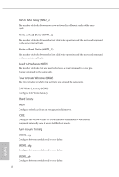
RAS to RAS Delay tRRD_L
 |
View all ASRock H410M-H/M.2 SE manuals
Add to My Manuals
Save this manual to your list of manuals |
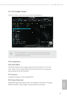
Page 47 highlights
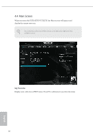
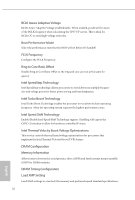
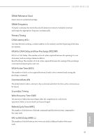
H410M-H/M.2 SE DRAM Reference Clock Select Auto for optimized settings. DRAM Frequency If [Auto] is selected, the motherboard will detect the memory module(s) inserted and assign the appropriate frequency automatically. Primary Timing CAS# Latency (tCL) The time between sending a column address to the memory and the beginning of the data in response. RAS# to CAS# Delay and Row Precharge (tRCDtRP) RAS# to CAS# Delay : The number of clock cycles required between the opening of a row of memory and accessing columns within it. Row Precharge: The number of clock cycles required between the issuing of the precharge command and opening the next row. RAS# Active Time (tRAS) The number of clock cycles required between a bank active command and issuing the precharge command. Command Rate (CR) The delay between when a memory chip is selected and when the first active command can be issued. Secondary Timing Write Recovery Time (tWR) The amount of delay that must elapse after the completion of a valid write operation, before an active bank can be precharged. Refresh Cycle Time (tRFC) The number of clocks from a Refresh command until the first Activate command to the same rank. RAS to RAS Delay (tRRD_L) The number of clocks between two rows activated in different banks of the same rank. 43 English
-
 1
1 -
2
-
3
-
4
-
5
-
6
-
7
-
8
-
9
-
10
-
11
-
12
-
13
-
14
-
15
-
16
-
17
-
18
-
19
-
20
-
21
-
22
-
23
-
24
-
25
-
26
-
27
-
28
-
29
-
30
-
31
-
32
-
33
-
34
-
35
-
36
-
37
-
38
-
39
-
40
-
41
-
 42
42 -
 43
43 -
 44
44 -
 45
45 -
 46
46 -
 47
47 -
 48
48 -
 49
49 -
 50
50 -
 51
51 -
 52
52 -
53
-
54
-
55
-
56
-
57
-
58
-
59
-
60
-
61
-
62
-
63
-
64
-
65
-
66
-
67
-
68
-
69
-
70
-
71
-
72
-
73
-
74
-
75
-
76
 |
 |
