ASRock P45TS User Manual - Page 22
Jumpers Setup - bios update
 |
View all ASRock P45TS manuals
Add to My Manuals
Save this manual to your list of manuals |
Page 22 highlights
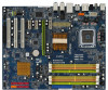
2.7 Jumpers Setup The illustration shows how jumpers are setup. When the jumper cap is placed on pins, the jumper is "Short". If no jumper cap is placed on pins, the jumper is "Open". The il- lustration shows a 3-pin jumper whose pin1 and pin2 are "Short" when jumper cap is placed on these 2 pins. Jumper Setting Description PS2_USB_PWR1 (see p.11/12 No. 1) 1_2 +5V 2_3 +5VSB Short pin2, pin3 to enable +5VSB (standby) for PS/2 or USB wake up events. Note: To select +5VSB, it requires 2 Amp and higher standby current provided by power supply. Clear CMOS Jumper (CLRCMOS1) (see p.11 No. 24 or p.12 No. 23) 1_2 2_3 Default Clear CMOS Note: CLRCMOS1 allows you to clear the data in CMOS. The data in CMOS includes system setup information such as system password, date, time, and system setup parameters. To clear and reset the system parameters to default setup, please turn off the computer and unplug the power cord from the power supply. After waiting for 15 seconds, use a jumper cap to short pin2 and pin3 on CLRCMOS1 for 5 seconds. However, please do not clear the CMOS right after you update the BIOS. If you need to clear the CMOS when you just finish updating the BIOS, you must boot up the system first, and then shut it down before you do the clearCMOS action. FSB1 Jumper (FSB1, 3-pin jumper, see p.11 No. 34 or p.12 No. 33) FSB2 Jumper (FSB2, 5-pin jumper, see p.11/12 No. 9) FSB3 Jumper (FSB3, 5-pin jumper, see p.11/12 No. 9) 1_2 FSB3 FSB2 1_2 FSB1 1_2 Default When you mount a FSB800 or FSB1066 CPU, and try to overclock to FSB1333 orFSB1600 (by BIOS setting) you may face the problem, that DRAM frequency will be overclocked very high. Please use jumper to force NB to be strapped at higher frequency, so the DRAM can work at lower frequency. 22
-
 1
1 -
2
-
3
-
4
-
5
-
6
-
7
-
8
-
9
-
10
-
11
-
12
-
13
-
14
-
15
-
16
-
 17
17 -
 18
18 -
 19
19 -
 20
20 -
 21
21 -
 22
22 -
 23
23 -
 24
24 -
 25
25 -
 26
26 -
 27
27 -
28
-
29
-
30
-
31
-
32
-
33
-
34
-
35
-
36
-
37
-
38
-
39
-
40
-
41
-
42
-
43
-
44
-
45
-
46
-
47
-
48
-
49
-
50
-
51
-
52
-
53
-
54
-
55
-
56
-
57
-
58
-
59
-
60
-
61
-
62
-
63
-
64
-
65
-
66
-
67
-
68
 |
 |
