ASRock P4i48 User Manual - Page 33
Con DRAM Timing by SPD
 |
View all ASRock P4i48 manuals
Add to My Manuals
Save this manual to your list of manuals |
Page 33 highlights
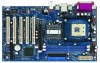
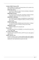
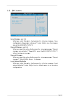
Configure DRAM Timing by SPD Select [Enabled] will configure the following items by the contents in the SPD (Serial Presence Detect) device. DRAM CAS# Latency Use this item to adjust the means of memory accessing. Configuration options: [Auto], [2.5], [2], and [3]. DRAM RAS# Precharge This controls the idle clocks after a precharge command is issued. Configuration options: [4 Clocks], [3 Clocks], and [2 Clocks]. DRAM RAS# to CAS# Delay This controls the latency between the DRAM active command and the read / write command. Configuration options: [4 Clocks], [3 Clocks], and [2 Clocks]. DRAM Precharge Delay This controls the number of DRAM clocks for RAS minimum. Configuration options: [8 Clocks], [7 Clocks], [6 Clocks], and [5 Clocks]. DRAM Burst Length DRAM Burst length can be set as [8] or [4]. Memory Hole The default value of this item is [Disabled], or you may set the value of this item as [15MB-16MB]. Init. Graphic Adapter Priority This allows you to select [PCI/AGP] or [AGP/PCI] as the initial graphics adapter priority. Graphics Aperture Size It refers to a section of the PCI memory address range used for graphics memory. It is recommended to leave this field at the default value unless the installed AGP card's specifications requires other sizes. 33
-
 1
1 -
2
-
3
-
4
-
5
-
6
-
7
-
8
-
9
-
10
-
11
-
12
-
13
-
14
-
15
-
16
-
17
-
18
-
19
-
20
-
21
-
22
-
23
-
24
-
25
-
26
-
27
-
 28
28 -
 29
29 -
 30
30 -
 31
31 -
 32
32 -
 33
33 -
 34
34 -
 35
35 -
 36
36
 |
 |