Asus A7Pro Motherboard DIY Troubleshooting Guide - Page 64
ASUS A7PRO User's Manual, SDRAM Configuration, SDRAM Con, figuration
 |
View all Asus A7Pro manuals
Add to My Manuals
Save this manual to your list of manuals |
Page 64 highlights
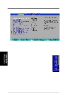
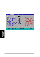
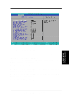
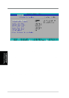
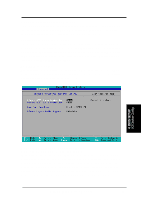
4. BIOS SETUP SDRAM Configuration [By SPD] This sets the optimal timings for SDRAM related fields, depending on the memory modules that you are using. Default setting is [By SPD], which configures the subsequent 3 items by reading the contents in the SPD (Serial Presence Detect) device. The EEPROM on the memory module stores critical parameter information about the module, such as memory type, size, speed, voltage interface, and module banks. Configuration options: [User Define] [7ns(143MHz)] [8ns(125MHz)] [By SPD] SDRAM CAS Latency This controls the latency between the SDRAM read command and the time that the data actually becomes available. NOTE: This field will only be adjustable when SDRAM Configuration is set to [User Define]. SDRAM RAS Precharge Time This controls the idle clocks after issuing a precharge command to the SDRAM. NOTE: This field will only be adjustable when SDRAM Configuration is set to [User Define]. SDRAM RAS to CAS Delay This controls the latency between the SDRAM active command and the read/write command. NOTE: This field will only be adjustable when SDRAM Configuration is set to [User Define]. PCI Master Read Caching Default: [Enabled] for Athlon Processors / [Disabled] for Duron Processors Leave on default setting. Configuration options: [Disabled] [Enabled] Delayed Transaction Default: [Enabled] for Athlon Processors / [Disabled] for Duron Processors Leave on default setting. Enabled, this frees the PCI Bus when the CPU is accessing 8-bit ISA devices that normally consume about 50-60 PCI Clocks without PCI delayed transaction. Select [Disabled] for ISA devices that are not PCI 2.1 compliant. Configuration options: [Disabled] [Enabled] PCI to DRAM Prefetch [Enabled] Configuration options: [Disabled] [Enabled] Byte Merge [Enabled] To optimize the data transfer on PCI, this merges a sequence of individual memory writes (bytes or words) into a single 32-bit block of data. However, byte merging may only be done when the bytes within a data phase are in a prefetchable address range. Configuration options: [Disabled] [Enabled] DRAM Read Latch Delay [Auto] Configuration options: [-0.01 ns] [0.75 ns]...[Auto] 4. BIOS SETUP Chip Configuration 64 ASUS A7PRO User's Manual
-
 1
1 -
2
-
3
-
4
-
5
-
6
-
7
-
8
-
9
-
10
-
11
-
12
-
13
-
14
-
15
-
16
-
17
-
18
-
19
-
20
-
21
-
22
-
23
-
24
-
25
-
26
-
27
-
28
-
29
-
30
-
31
-
32
-
33
-
34
-
35
-
36
-
37
-
38
-
39
-
40
-
41
-
42
-
43
-
44
-
45
-
46
-
47
-
48
-
49
-
50
-
51
-
52
-
53
-
54
-
55
-
56
-
57
-
58
-
 59
59 -
 60
60 -
 61
61 -
 62
62 -
 63
63 -
 64
64 -
 65
65 -
 66
66 -
 67
67 -
 68
68 -
 69
69 -
70
-
71
-
72
-
73
-
74
-
75
-
76
-
77
-
78
-
79
-
80
-
81
-
82
-
83
-
84
-
85
-
86
-
87
-
88
-
89
-
90
-
91
-
92
-
93
-
94
-
95
-
96
-
97
-
98
-
99
-
100
-
101
-
102
-
103
-
104
 |
 |