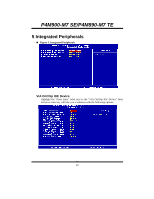
Biostar P4M890-M7 TE Bios Setup - Page 20
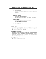
Memory Hole, System BIOS Cacheable, Top Performance
 |
View all Biostar P4M890-M7 TE manuals
Add to My Manuals
Save this manual to your list of manuals |
Page 20 highlights
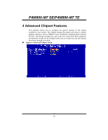
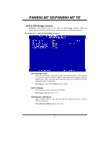
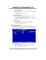
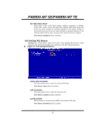
P4M900-M7 SE/P4M890-M7 TE PCI Delay Transaction The chipset has an embedded 32-bit posted write buffer to support delay transactions cycles. Select Enabled to support compliance with PCI specification. The Choices: Enabled (default), Disabled. VLink mode selection This item allows you to select Vlink mode. The Choices: By Auto (default), Mode 0 , Mode 1, Mode 2, Mode 3, Mode 4. VLink 8X Support This item allows you to enable or disable VLink 8X support. The Choices: Enabled (default), Disabled. VIA PWR Management The Choices: Enabled (default), Disabled. Memory Hole You can reserve this area of system memory for ISA adapter ROM. When this area is reserved it cannot be cached. Check the user information of peripherals that need to use this area of system memory for the memory requirements. The Choices: Disabled (default), 15M-16M. System BIOS Cacheable Selecting the "Enabled" option allows caching of the system BIOS ROM at F0000h-FFFFFh, which is able to improve the system performance. However, any programs that attempts to write to this memory block will cause conflicts and result in system errors. The Choices: Enabled (default), Disabled. Top Performance The Choices: Disabled (default), Enabled. 19
-
 1
1 -
2
-
3
-
4
-
5
-
6
-
7
-
8
-
9
-
10
-
11
-
12
-
13
-
14
-
 15
15 -
 16
16 -
 17
17 -
 18
18 -
 19
19 -
 20
20 -
 21
21 -
 22
22 -
 23
23 -
 24
24 -
 25
25 -
26
-
27
-
28
-
29
-
30
-
31
-
32
-
33
-
34
-
35
-
36
-
37
-
38
-
39
-
40
 |
 |
