Dell 2005FPW Service Manual - Page 10
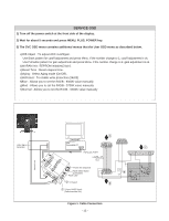
Description Of Block Diagram - panel
 |
UPC - 012345698705
View all Dell 2005FPW manuals
Add to My Manuals
Save this manual to your list of manuals |
Page 10 highlights
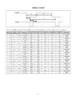
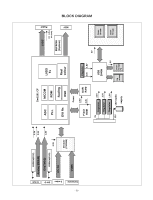
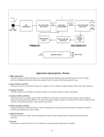
DESCRIPTION OF BLOCK DIAGRAM 1. Video Controller Part & Display Data Transmitter Part. This part amplifies the level of video signal for the digital conversion and converts from the analog video signal to the digital video signal using a pixel clock. The pixel clock for each mode is generated by the PLL. The range of the pixel clock is from 25MHz to 147MHz. This part consists of the Scaler, Flash-ROM IC which stores program data, Reset IC. The Scaler gets the video signal converted analog to digital, interpolates input to 1680 x1050 resolution signal and outputs 8-bit R, G, B signal to transmitter. Especially pre-amp / ADC / Video controller/ Transmitter are merged to one chip "Gm1501" by Genesis. This part transmit digital signal from the Scaler to the receiver of module.s 2. Power Part This part consists of the two 3.3V and one 2.5V and one 1.8Vregulators to convert power which is provided 12V in Power Board V is provided for LCD Panel.(Only LPL) 5V in Power Board V is provided for LCD Panel.(Only AUO) 12V in Power Board V is provided for Inverter Part. Also, 5V is converted 3.3V and 2.5V and 1.8V by regulator. Converted power is provided for IC in the main board. - 10 -
-
 1
1 -
2
-
3
-
4
-
 5
5 -
 6
6 -
 7
7 -
 8
8 -
 9
9 -
 10
10 -
 11
11 -
 12
12 -
 13
13 -
 14
14 -
 15
15 -
16
-
17
-
18
-
19
-
20
-
21
-
22
-
23
-
24
-
25
-
26
-
27
-
28
-
29
-
30
-
31
-
32
-
33
 |
 |