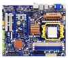
Foxconn A7DA-S English Manual. - Page 43
► Power Down Enable, ► Power Down Mode, ► DRAM Timing Mode, ► CAS Latency - tCL
 |
View all Foxconn A7DA-S manuals
Add to My Manuals
Save this manual to your list of manuals |
Page 43 highlights
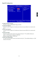
3 Burst lengths supported When both DCTs are enabled in unganged mode, BIOS must initialize the frequency of each DCT in order. ► Power Down Enable When power down mode is enabled, if all pages of the DRAMs associated with a CKE pin are closed, then these parts are placed in power down mode. ► Power Down Mode For non-mobile systems, power down mode should be set to [Channel] CKE control. A DIMM or a group of DIMMs enters power down mode by deasserting the corresponding clock enable signal when the DRAM controller detects that there are no transactions scheduled to any of the DIMMs connected to the clock enable signal. A DIMM or a group of DIMMs exits power down mode by asserting the corresponding clock enable signal when a transaction is scheduled to any DIMM connected to the clock enable signal. There are two CKE pins per DRAM channel. For each channel : [Channel] CKE control. The DRAM channel is placed in power down when all chip selects associated with the channel are idle. [Chip Select] CKE control. A chip select or pair of chip selects is placed in power down when no transactions are pending for the chip select(s). DRAM Timing Configuration CMOS Setup Utility - Copyright (C) 1985-2006, American Megatrends, Inc. DRAM Timing Configuration DRAM Timing Configuration DRAM Timing Mode [Auto] Help Item Options Auto DCT0 Move Enter:Select +/-/:Value F10:Save ESC:Exit F1:General Help F9:Optimized Defaults ► DRAM Timing Mode When both DCTs (DRAM controller) are enabled in unganged mode, BIOS must initialize the frequency of each DCT in order. Settings are : [Auto]; [DCT 0]. (appear in AM2 CPU) Settings are : [Auto]; [DCT 0]; [DCT1]; [Both]. (appear in AM2+ CPU) ► CAS Latency - tCL The number of memory clocks it takes a DRAM to return data after the read CAS_L is asserted depends on the memory clock frequency. The value that BIOS programs into the memory 36
-
 1
1 -
2
-
3
-
4
-
5
-
6
-
7
-
8
-
9
-
10
-
11
-
12
-
13
-
14
-
15
-
16
-
17
-
18
-
19
-
20
-
21
-
22
-
23
-
24
-
25
-
26
-
27
-
28
-
29
-
30
-
31
-
32
-
33
-
34
-
35
-
36
-
37
-
 38
38 -
 39
39 -
 40
40 -
 41
41 -
 42
42 -
 43
43 -
 44
44 -
 45
45 -
 46
46 -
 47
47 -
 48
48 -
49
-
50
-
51
-
52
-
53
-
54
-
55
-
56
-
57
-
58
-
59
-
60
-
61
-
62
-
63
-
64
-
65
-
66
-
67
-
68
-
69
-
70
-
71
-
72
-
73
-
74
-
75
-
76
-
77
-
78
-
79
-
80
-
81
-
82
-
83
-
84
-
85
-
86
-
87
-
88
-
89
-
90
-
91
-
92
-
93
-
94
-
95
-
96
-
97
-
98
-
99
-
100
-
101
-
102
-
103
-
104
-
105
-
106
-
107
-
108
-
109
-
110
-
111
 |
 |
