Foxconn Z68A-S Manual - Page 35
Chipset Performance Tuning
 |
View all Foxconn Z68A-S manuals
Add to My Manuals
Save this manual to your list of manuals |
Page 35 highlights
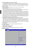
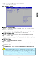
Chipset Performance Tuning Aptio Setup Utility - C opyright (C) 2011 American Megatrends, Inc. Advanced Memory Multiplier Configuration Memory Multiplier Memory Multiplier [13.33] Memory Timing Configuration CAS# Latency(tCL) 9 Row Precharge Time(tRP) 9 RAS# to CAS# Delay(tRCD) 9 RAS# Active Time(tRAS) 24 Write Recovery Time(tWR) 10 Row Refresh Cycle Time(tRFC) 74 Write to Read Delay(tWTR) 5 Active to Active Delay(tRRD) 4 Read CAS# Precharege(tRTP) 5 Four Active Window Delay(tFAW) 20 Intel Graphics Configuration Graphics Core Ratio Limit 22 Graphics Voltage(1/10000) 0 → ←: Select Screen ↑ ↓: Select Item Enter: Select +/-: Change Opt. F1: General Help F2: Previous Values F3: Optimized Defaults F4: Save & Exit ESC: Exit 3 Version 2.10.1208. Copyright (C) 2011 American Megatrends, Inc. ► Memory Multiplier This item is used to adjust the memory Clock Ratio. The available settimgs are: [Auto], [10.67], [13.33], [16], [18.67], [21.33]. ► CAS# Latency (tCL) The number of memory clocks it takes a DRAM to return data after the read CAS_L is asserted depends on the memory clock frequency. The value that BIOS programs into the memory controller is a function of the target clock frequency. The target clock frequency is determined from the supported CAS latencies at given clock frequencies of each DIMM. ► Row Precharge Time (tRP) This item allows you to select the row precharge time (in clock cycles). ► RAS# to CAS# Delay (tRCD) This item allows you to select a delay time (in clock cycles) between the CAS# and RAS# strobe signals. ► RAS# Active Time (tRAS) This item allows you to set the minimum RAS# active time (in clock cycles). ► Write Recovery Time (tWR) This item allows you to select the write recovery time (in clock cycles). ► Row Refresh Cycle Time (tRFC) Refresh to Refresh or Refresh to Active command interval. ► Write to Read Delay (tWTR) This item allows you to select a delay time (in clock cycles) between sending the last data from a write operation to the memory and issuing a read command. ► Active-to-Active Delay (tRRD) This item allows you to select a delay time (in clock cycles) between the RAS# and RAS# strobe signals. 28
-
 1
1 -
2
-
3
-
4
-
5
-
6
-
7
-
8
-
9
-
10
-
11
-
12
-
13
-
14
-
15
-
16
-
17
-
18
-
19
-
20
-
21
-
22
-
23
-
24
-
25
-
26
-
27
-
28
-
29
-
 30
30 -
 31
31 -
 32
32 -
 33
33 -
 34
34 -
 35
35 -
 36
36 -
 37
37 -
 38
38 -
 39
39 -
 40
40 -
41
-
42
-
43
-
44
-
45
-
46
-
47
-
48
-
49
-
50
-
51
-
52
-
53
-
54
-
55
-
56
-
57
-
58
-
59
-
60
-
61
-
62
-
63
-
64
-
65
-
66
-
67
-
68
-
69
-
70
-
71
-
72
-
73
-
74
-
75
-
76
-
77
-
78
-
79
-
80
-
81
-
82
-
83
-
84
-
85
-
86
-
87
-
88
-
89
-
90
-
91
-
92
-
93
-
94
-
95
-
96
-
97
-
98
-
99
-
100
-
101
-
102
-
103
-
104
-
105
-
106
-
107
-
108
-
109
-
110
-
111
-
112
-
113
-
114
-
115
-
116
-
117
-
118
-
119
-
120
-
121
-
122
-
123
-
124
-
125
-
126
-
127
-
128
-
129
 |
 |