Gigabyte GA-890XA-UD3 Manual - Page 8
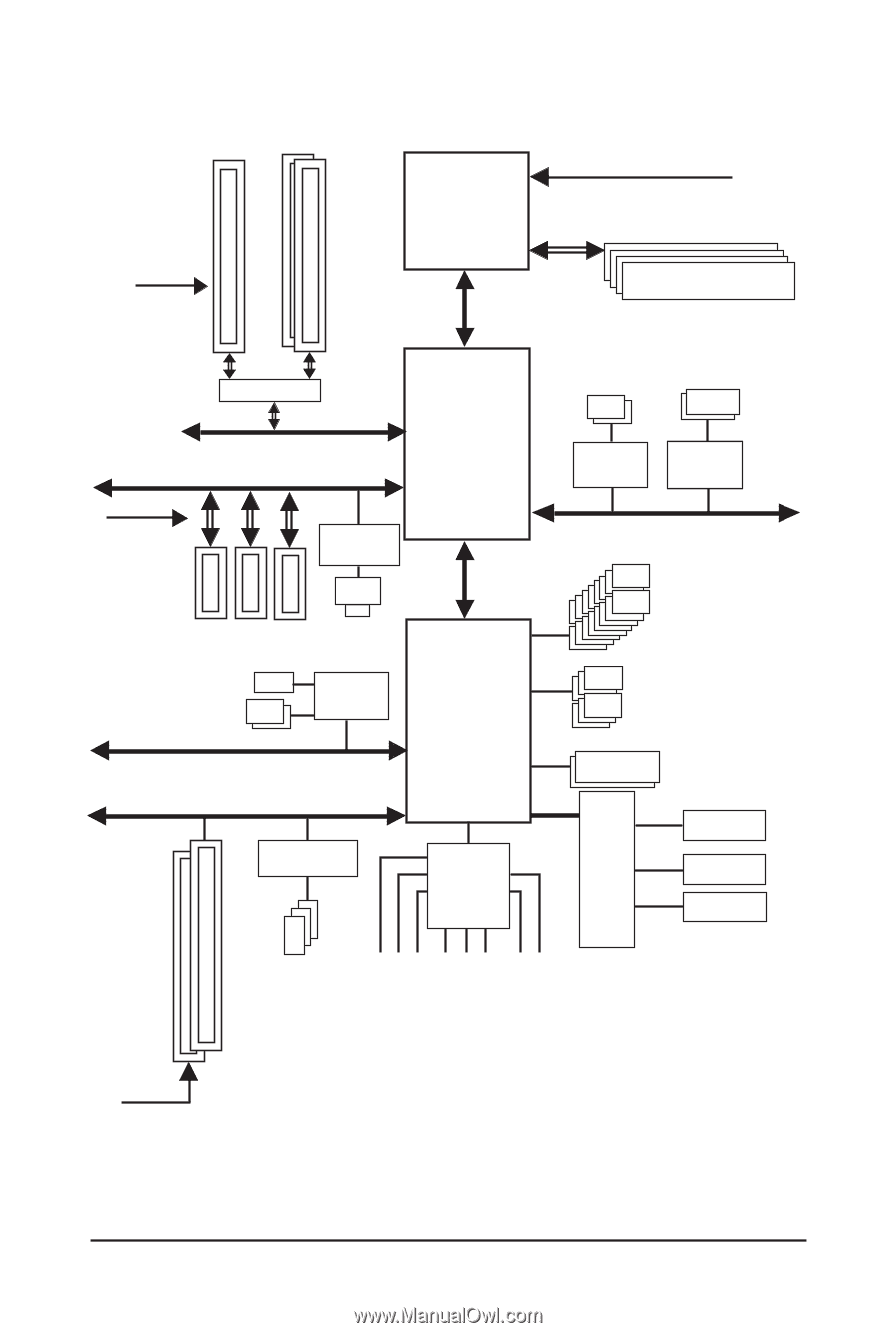
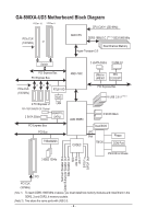
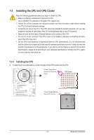
GA-890XA-UD3 Motherboard Block Diagram - socket am3
 |
UPC - 818313010315
View all Gigabyte GA-890XA-UD3 manuals
Add to My Manuals
Save this manual to your list of manuals |
Page 8 highlights
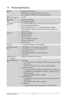
GA-890XA-UD3 Motherboard Block Diagram 1 PCIe x 16 2 PCIe x 8 CPU CLK+/- (200 MHz) PCIe CLK (100 MHz) or AM3 CPU DDR3 1866(O.C.)(Note 1)/1333/1066 MHz Dual Channel Memory Hyper Transport 3.0 Switch 2 eSATA 3Gb/s 2 USB 3.0 PCI Express Bus PCI Express Bus PCIe CLK (100 MHz) x1 x1 x1 RTL8111D RJ45 3 PCI Express x1 LAN ATA-133/100/66/33 IDE Channel 2 SATA 3Gb/s GIGABYTE SATA2 PCI Express Bus PCI Bus TSB43AB23 AMD 790X AMD SB850 CODEC JMicron NEC JMB362 D720200F1 PCI Express Bus 16 USB 2.0/1.1(Note 2) 6 SATA 6Gb/s Dual BIOS LPC Bus IT8720 Floppy COM Port 3 IEEE 1394a PS/2 KB or Mouse Surround Speaker Out Center/Subwoofer Speaker Out Side Speaker Out MIC Line Out Line In S/PDIF In S/PDIF Out 2 PCI 2 PCI PCI CLK (33 MHz) (Note 1) To reach DDR3 1866 MHz or above, you must install two memory modules and install them in the DDR3_3 and DDR3_4 memory sockets. (Note 2) Two share the same ports with USB 3.0. - 8 -
-
 1
1 -
2
-
 3
3 -
 4
4 -
 5
5 -
 6
6 -
 7
7 -
 8
8 -
 9
9 -
 10
10 -
 11
11 -
 12
12 -
 13
13 -
14
-
15
-
16
-
17
-
18
-
19
-
20
-
21
-
22
-
23
-
24
-
25
-
26
-
27
-
28
-
29
-
30
-
31
-
32
-
33
-
34
-
35
-
36
-
37
-
38
-
39
-
40
-
41
-
42
-
43
-
44
-
45
-
46
-
47
-
48
-
49
-
50
-
51
-
52
-
53
-
54
-
55
-
56
-
57
-
58
-
59
-
60
-
61
-
62
-
63
-
64
-
65
-
66
-
67
-
68
-
69
-
70
-
71
-
72
-
73
-
74
-
75
-
76
-
77
-
78
-
79
-
80
-
81
-
82
-
83
-
84
-
85
-
86
-
87
-
88
-
89
-
90
-
91
-
92
-
93
-
94
-
95
-
96
-
97
-
98
-
99
-
100
-
101
-
102
-
103
-
104
-
105
-
106
-
107
-
108
-
109
-
110
-
111
-
112
 |
 |