Gigabyte GA-H55-UD3H Manual - Page 8
Block Diagram - h55
 |
View all Gigabyte GA-H55-UD3H manuals
Add to My Manuals
Save this manual to your list of manuals |
Page 8 highlights
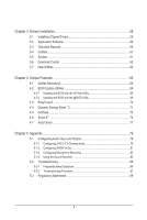
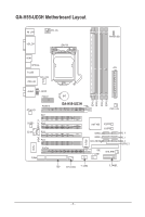
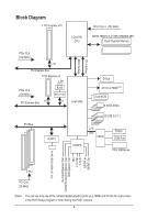
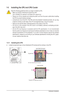
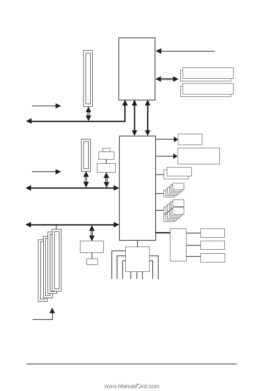
Block Diagram 1 PCI Express x16 LGA1156 CPU CPU CLK+/- (133 MHz) DDR3 1666(O.C.)/1333/1066/800 MHz Dual Channel Memory PCIe CLK (100 MHz) x16 PCI Express Bus 1 PCI Express x4 LAN PCIe CLK (100 MHz) RJ45 RTL8111D PCI Express Bus x4 x1 Intel® H55 FDI Interface DMI Interface D-Sub DVI-D or HDMI (Note) Dual BIOS 6 SATA 3Gb/s PCI Bus IT8213 12 USB 2.0/1.1 CODEC LPC Bus IT8720 Floppy COM Port PS/2 KB/Mouse ATA-133/100/66/33 IDE Channel Surround Speaker Out Center/Subwoofer Speaker Out Side Speaker Out MIC Line Out Line In S/PDIF In S/PDIF Out 4 PCI PCI CLK (33 MHz) (Note) You can use only one of the onboard digital graphics ports (e.g. HDMI and DVI-D) for output when in the BIOS Setup program or when during the POST screens. - 8 -
-
 1
1 -
2
-
 3
3 -
 4
4 -
 5
5 -
 6
6 -
 7
7 -
 8
8 -
 9
9 -
 10
10 -
 11
11 -
 12
12 -
 13
13 -
14
-
15
-
16
-
17
-
18
-
19
-
20
-
21
-
22
-
23
-
24
-
25
-
26
-
27
-
28
-
29
-
30
-
31
-
32
-
33
-
34
-
35
-
36
-
37
-
38
-
39
-
40
-
41
-
42
-
43
-
44
-
45
-
46
-
47
-
48
-
49
-
50
-
51
-
52
-
53
-
54
-
55
-
56
-
57
-
58
-
59
-
60
-
61
-
62
-
63
-
64
-
65
-
66
-
67
-
68
-
69
-
70
-
71
-
72
-
73
-
74
-
75
-
76
-
77
-
78
-
79
-
80
-
81
-
82
-
83
-
84
-
85
-
86
-
87
-
88
-
89
-
90
-
91
-
92
-
93
-
94
-
95
-
96
 |
 |
- 8 -
Block Diagram
(Note)
You can use only one of the onboard digital graphics ports (e.g. HDMI and DVI-D) for output when
in the BIOS Setup program or when during the POST screens.
Center/Subwoofer Speaker Out
Line Out
MIC
Line In
S/PDIF In
S/PDIF Out
Side Speaker Out
Surround Speaker Out
CODEC
PS/2 KB/Mouse
LGA1156
CPU
DMI Interface
4 PCI
PCI Bus
PCI CLK
(33 MHz)
PCIe CLK
(100 MHz)
PCI Express Bus
IT8720
Floppy
CPU CLK+/- (133 MHz)
6 SATA 3Gb/s
1 PCI Express x16
Dual BIOS
COM Port
12 USB 2.0/1.1
LPC
Bus
ATA-133/100/66/33 IDE Channel
IT8213
DDR3 1666(O.C.)/1333/1066/800 MHz
Dual Channel Memory
x1
LAN
RJ45
RTL8111D
x4
1 PCI Express x4
PCI Express Bus
x16
PCIe CLK
(100 MHz)
D-Sub
FDI Interface
Intel
®
H55
DVI-D or HDMI
(Note)