Intel D865PCK D865PCK Technical Product Specification - Page 32
DMA Channels, 4 Fixed I/O Map
 |
View all Intel D865PCK manuals
Add to My Manuals
Save this manual to your list of manuals |
Page 32 highlights
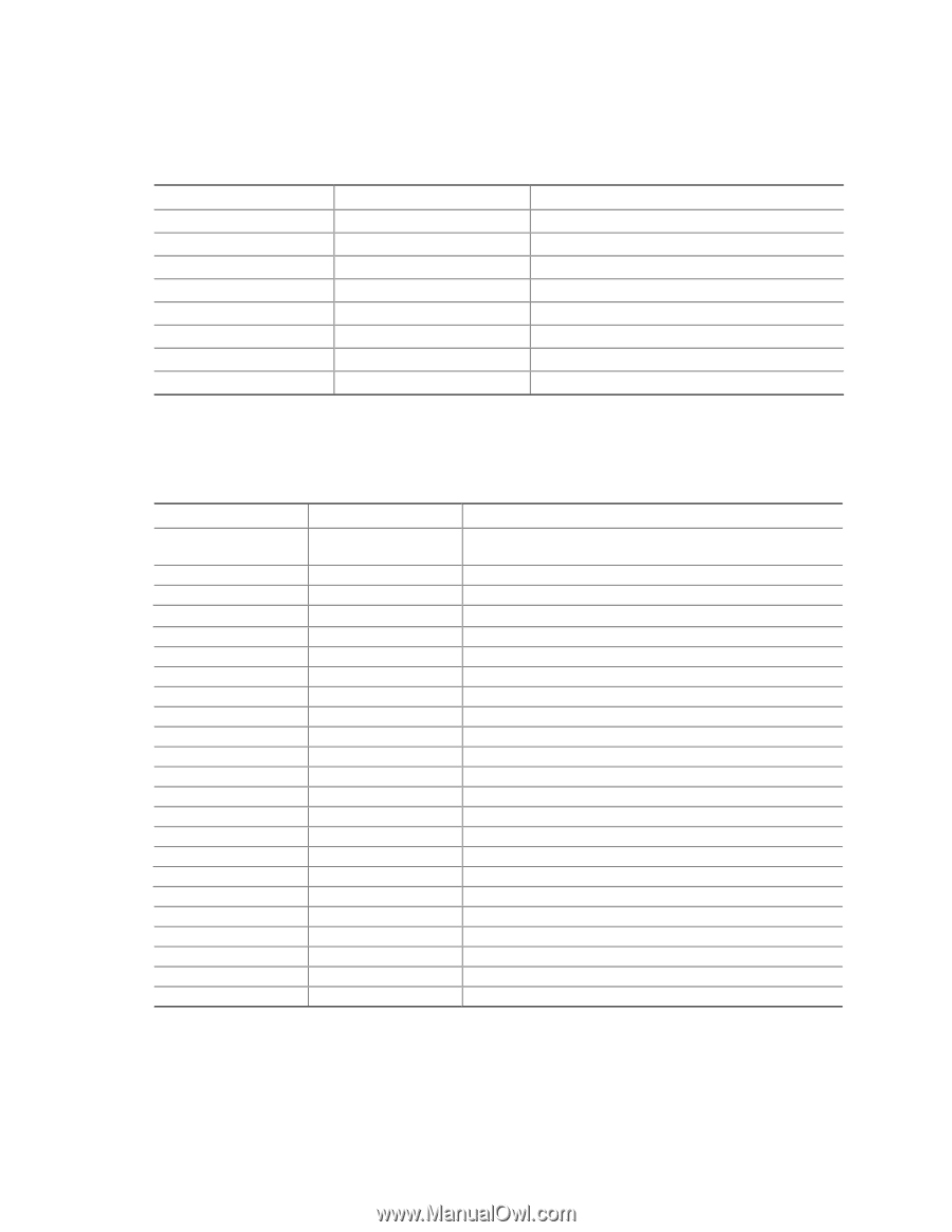
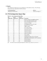
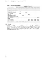
Intel Desktop Board D865PCK Technical Product Specification 2.3 DMA Channels Table 10. DMA Channels DMA Channel Number 0 1 2 3 4 5 6 7 Data Width 8 or 16 bits 8 or 16 bits 8 or 16 bits 8 or 16 bits 8 or 16 bits 16 bits 16 bits 16 bits System Resource Open Parallel port Diskette drive Parallel port (for ECP or EPP) DMA controller Open Open Open 2.4 Fixed I/O Map Table 11. I/O Map Address (hex) Size Description 0000 - 00FF 0170 - 0177 01F0 - 01F7 256 bytes 8 bytes 8 bytes Used by the Desktop Board D865PCK. Refer to the ICH5 data sheet for dynamic addressing information. Secondary Parallel ATA IDE channel command block Primary Parallel ATA IDE channel command block 0228 - 022F (Note 1) 0278 - 027F (Note 1) 02E8 - 02EF (Note 1) 02F8 - 02FF (Note 1) 8 bytes 8 bytes 8 bytes 8 bytes LPT3 LPT2 COM4 COM2 0374 - 0377 0377, bits 6:0 0378 - 037F 03B0 - 03BB 03C0 - 03DF 03E8 - 03EF 03F0 - 03F5 4 bytes 7 bits 8 bytes 12 bytes 32 bytes 8 bytes 6 bytes Secondary Parallel ATA IDE channel control block Secondary IDE channel status port LPT1 Intel 82865P MCH Intel 82865P MCH COM3 Diskette channel 03F4 - 03F7 03F8 - 03FF 04D0 - 04D1 LPTn + 400 0CF8 - 0CFB (Note 2) 0CF9 (Note 3) 0CFC - 0CFF FFA0 - FFA7 FFA8 - FFAF 1 byte 8 bytes 2 bytes 8 bytes 4 bytes 1 byte 4 bytes 8 bytes 8 bytes Primary Parallel ATA IDE channel control block COM1 Edge/level triggered PIC ECP port, LPTn base address + 400h PCI configuration address register Reset control register PCI configuration data register Primary Parallel ATA IDE bus master registers Secondary Parallel ATA IDE bus master registers Notes: 1. Default, but can be changed to another address range 2. Dword access only 3. Byte access only 32
-
 1
1 -
2
-
3
-
4
-
5
-
6
-
7
-
8
-
9
-
10
-
11
-
12
-
13
-
14
-
15
-
16
-
17
-
18
-
19
-
20
-
21
-
22
-
23
-
24
-
25
-
26
-
 27
27 -
 28
28 -
 29
29 -
 30
30 -
 31
31 -
 32
32 -
 33
33 -
 34
34 -
 35
35 -
 36
36 -
 37
37 -
38
-
39
-
40
-
41
-
42
-
43
-
44
-
45
-
46
-
47
-
48
-
49
-
50
-
51
-
52
-
53
-
54
-
55
-
56
-
57
-
58
-
59
-
60
-
61
-
62
-
63
-
64
-
65
-
66
-
67
-
68
-
69
-
70
-
71
-
72
-
73
-
74
-
75
-
76
 |
 |