LG 50PJ340 Training Manual - Page 130
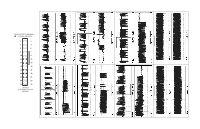
Circuit Interconnect Diagram, Connect Scope between Waveform, TP on Y-Drive and Gnd
 |
View all LG 50PJ340 manuals
Add to My Manuals
Save this manual to your list of manuals |
Page 130 highlights
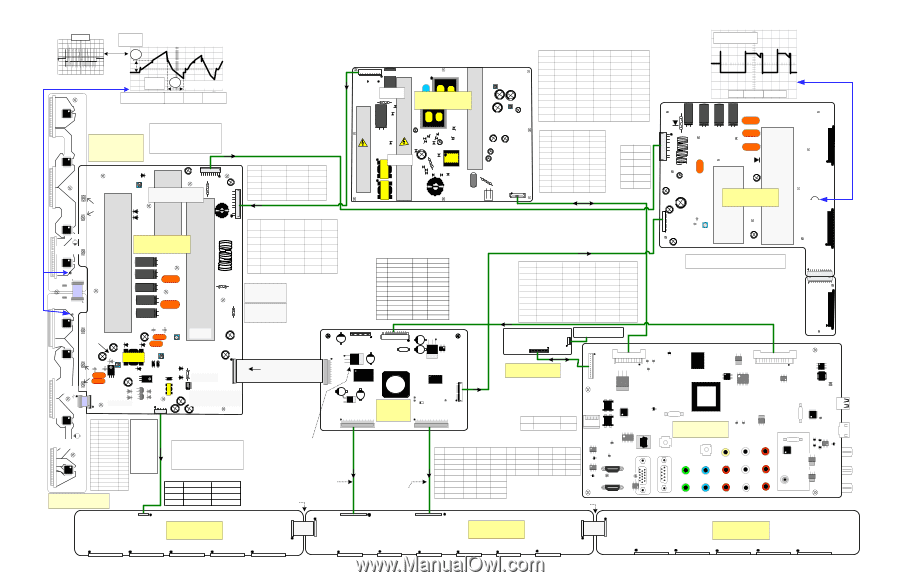
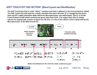
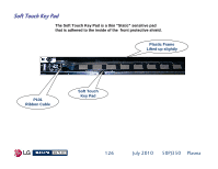
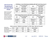
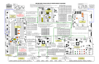
2mS VR402 Set-up 224V p/p ± 5V A 0V VS-DA on the control PWB can be used as a trigger for Y or Z-SUS. VR401 B Set-Dn 180uSec ± 5uSec 50PJ350 (50T1 Panel) CIRCUIT INTERCONNECT DIAGRAM SMPS Stand-Alone Test - Unplug P813 to Main board. Use two (100W) light bulbs in series between Vs and Gnd to place a load on the SMPS. Apply AC, all voltage should run. To Test the Set without Main board, leave P812 connected. Do not use light bulbs. See "Auto Gen" on the Control board to perform a Panel Test. If all supplies do not run when A/C is applied, disconnect P812 to isolate the excessive load. P813 "SMPS" to P301 "Main" Pin Label STBY Run 1~2 16V 0V 17V 3~4 Gnd Gnd Gnd No Load Diode 17V 3.17V Gnd Gnd VA TP P812 VS TP 5~7 5V 0.46V 5.17V 5.19V 1.13V T901 VS 8 Error_Det 2.85V 4.9V 4.9V 3.0V ADJ 9~12 Gnd Gnd Gnd Gnd Gnd 75VAC rms "White" 90VAC rms "Black" 100V 100uS 548V p/p Step 1: RL_On command turns on the 17V, F801 4A 250V Stand-By: 0.9V Run: 388V ZD803 SMPS p/n: EAY60968701 13~14 STBY_5V 15 RL_ON 16 AC Det 3.46V 0V 0V 5.14V 2.43V 4.44V 5.19V 0V 4.92V 2.56V Open 3.1V IC110 P101 IC120 P102 Connect Scope between Waveform TP on Y-Drive and Gnd Y-DRIVE UPPER BOARD p/n: EBR63551601 WARNING: Remove upper Y-DRIVE Board completely if P110 or P204 is removed. +5V, AC-Det and Error_Det. If Missing, the set will Shut Off after 10 Seconds. Error_Det. is not used by the Main. Step 2: M5 On command Turns on M5V, then Va, then Vs. Floating GND D401 SET-UP VR402 D409 FS203 VS Diode Check reads Open with Board Disconnected or Connected P211 FS203 4A VS P211 "Y-SUS" to "Z-SUS" P2 Pin Label Run Diode 1~2 Gnd Gnd Gnd 3 n/c n/c n/c 4~5 +Vs *206V Open 6 n/c n/c n/c 7~11 ER_PASS 98V~102V Open D805 T902 D601 ZD302 D609 ZD401 D307 ZD301 ZD101 ZD303 D601 D303 D305 Stand-By: 1.5V Run: 388V L601 D308 D309 D306 F302 2.5A 250V D302 T301 D103 D301 L602 F101 10A 250V SC101 VA ADJ P813 17 M_ON 0V 18 Auto_Gnd Gnd 3.29V 0V Gnd 4.84V Open Open P1 "Z-SUS Board" to "Control" P101 Pin *1~2 *3~4 5 Label (+15V) (+15V) Gnd Run Diode 16V Open 16V Open Gnd Gnd P2 "Z-SUS" to "Y-SUS" P111 Pin Diode 6 Y_OE 0.058V Open 1~2 Gnd 7 ZBIAS 1.83V 2.82V 8 Slope_Ctl 0.086V 2.82V 9 Z_ER 0.14V 2.82V 3 n/c 4~5 Open 10 ZSUS_DN 0.77V 2.82V 6 n/c 11 ZSUS_UP 0.17V 2.82V 12 Gnd Gnd Gnd 7~11 Open * If 16V is missing check FS204 on the Y-Sus. IC130 C105 D407 Y-SUS P210 P210 "Y-SUS" to "SMPS" P812 Pin Label 1~2 VS 3 n/c Run *195V n/c P210 P812 Diode Diode Open Open n/c n/c a Note: The RL_On turns on +5V, 17V Error Det. and AC_DET. b Note: The M5-On command turns on M5V, Va and Vs. c Note: The Error Det line is not used in this model. d Note: If the AC Det line is Missing, the TV will turn off in 10 Seconds. e Note: Pin 18 is grounded on the Main. If opened, the power If AC-Det is missing, as a work around test, Jump the STBY-5V to the AC-Det line. If the set works normally, then the SMPS is defective. If the Main board is the problem, perform the normal Panel Test to confirm the Main is the only problem. 50VAC rms "White" 46VAC rms "Black" FS1 Diode Check Open with Board Connected or Disconnected 50V 100uS 248V p/p 250V FS1 220uf 250V 220uf 250V 220uf 250V 220uf D309 P2 D312 VZB TP + P1 - VR201 Z-SUS p/n: EBR63040301 Connect Scope between Waveform TP J36 on Z board and Gnd. Use RMS information just to check for board activity. VS-DA on the control PWB can be used as a trigger for Y or Z-SUS. P101 J36 Z-SUS OUT TP P102 Test FG5V across C105 IC140 Scan p/n: EBR63039801 250V 220uf 4~5 Gnd 6~7 VA 8 Gnd Gnd *60V Gnd Gnd Open Gnd Gnd Open Gnd supply turns on automatically. P101 Connector "Control" to "Z-SUS Board" P1 Pin Label Run Diode 1 (+15V) 16V Open Z-Drive Creation Signals P301 "Main" to "SMPS" P813 Pin Label STBY P108 P103 N/C Y Signal TP P110 250V 220uf 250V 220uf FS201 10A VA 9~10 M5V 5.1V FS201 Va Diode Check reads Open 1.19V 2.1V 2 (+15V) 16V Open 3 (+5V) 4.9V 1.52V 4 (+5V) 4.9V 1.52V 5 Gnd Gnd Gnd 6 Y_OE 0.058V 3.09V 1~2 16V 0V 3~4 Gnd Gnd 5~7 5V 0.46V 8 Error_Det 2.85V P209 P201 N/C P204 Y Signal TP 250V 220uf 250V 220uf FS202 10A 5VDC with Board Disconnected 7 ZBIAS 1.83V Open or Connected Control Board Test 8 Slop_Ctl Gnd Open FS202 M5V Diode Check reads 0.97V Board Connected or 1.19 Disconnected With the unit on, if D201 is not on, check 5V supply from FS202 on the Y-SUS. Also on pins 4~7 of P111. If present replace the Control Board. If missing, 9 10 11 12 Z_ER ZSUS_DN ZSUS_UP Gnd 0.14V 0.77V 0.17V Gnd Open Open Open Gnd 9~12 13~14 15 16 17 Gnd STBY_5V RL_ON AC Det M_ON Gnd 3.46V 0V 0V 0V -VY See (To Test Control Board) IC201 IC202 Scan ZD501 Feed Back ref for VSC regulation D504 VSC TP Floating GND ZD501 T302 VSC Anti PRV D502 TP SET-DN ZD502 FB ref for 15VFG VR401 D503 IC503 -VYVR5G02rayaerde out on components the back D501 IC502 FS204 2A 16VDC P101 IC302 D515 Cathode 1~3 (16V) 4-7 (M5V) Ribbon Cable Y-SUS and Y Drive Signals P102 IC231 P111 IC101 P121 X101 IC231 (1) Gnd (2) 3.29V (3) 4.94V IC141 IC211 IC211 (1) Gnd (2) 1.8V IC101(3) 3.27V Ft IR Intelligent Sensor P100 P101 IR Board p/n: EBR65007704 Q502 Q503 Source for +16V FG5V FL201 P205 P202 IC203 C205 Test FG5V across C205 P203 IC204 Anode = 15VFG IC508 2 D513 31 D511 P212 D514 21 3 Anode = 5VFG IC509 D512 P203 P212 "Y-SUS" to P205 Pin Label Run 1 SUS_DN (FG) 0V 2 FG5V 4.9V Note: Connectors D515 T502 IC510 D504 Cathode Source for VSC D503 Cathode Source for -Vy D512 Cathode Source for 5VFG D511 Cathode Source for 15VFG FS204 Protects 16V Creation D501 and IC501. Diode Check 1.61V With Board Disconnected or 1.59V Connected Note: IC231 (3.3V Regulator) routed to all X Boards To Check for Y-SUS Drive Waveform With the Y-Drive boards Disconnected IC801 (1) 1.79V (2) 3.29V IC801 (3) n/c (4) 0V (5) 0V P161 IC1 CONTROL BOARD p/n: EBR63549501 Auto Gen P101 D201 LED VS_DA 3.3V from IC231 Pins 56~60 P162 PANEL TEST: Disconnect P301, Remove LVDS Cable. Short across Auto Gen TPs to generate a test pattern. When A/C power is applied. Measuring Voltage on Pin 1 of P101 with DVM turns the TV on. If TV is on, Input Menu pops up. P101 (Ft IR) to Key Pad Pin Stby/Run Diode 1~8 0.07V/0.16V 2.4V 3 FG5V 4.9V 4 SUS_DN (FG) 0V 5 SUS_DN (FG) 0V 6 YB_CLK 0.86V between P212~P205 and Use the 3rd screw on the left from the bottom. WARNING: To Test Control Board: Disconnect all connectors. Jump STBY 5V from SMPS P813 Pin 13 to pin * If the complaint is no video and P704 "Main" to P100 (Ft IR) 7 YB_CLK 0.86V P204~P110 8 YB_STB 2.8V 9 YB_STB 2.8V 10 YTB_OC1 2.2V 11 YTB_OC1 2.2V DO NOT come with a new 12 YT_DATA 0V board Va Remove lower Y-DRIVE Board completely if P212 or P205 is removed. 3 (bottom leg) of IC231. Apply AC and turn on the Set. Observe Control board LED D201, if it's on, most likely Control board is OK. shorting the points (AutoGen) causes video to appear suspect the Main board or LVDS cable. Note: LVDS Cable must be removed for Auto Gen to work. Pin Label 1 IR 2 Gnd 3 Key 1 STBY Run 3.3V 3.76V Gnd Gnd 3.3V 3.29V Diode 3.12V Gnd 1.53V Pin Label STBY Run Diode 9 Gnd Gnd Gnd Gnd 10 3.3V_ST 3.3V 3.29V 0.85V 11 3.3V_MST 0V 3.31V 0.50V 13 YT_DATA 0V 4 Key 2 3.3V 3.29V 1.53V 12 LED Blue 0V 0V Open 14 YB_OC2 2.63V 15 YB_OC2 2.63V 16 SUS_DN (FG) FG 17 SUS_DN (FG) FG P203 "Y-SUS" and P122 "X-Left" Pin 1,2,3 Run Gnd Diode Check Gnd X-Drive Center and Left RGB Signals 3.3V and X-Drive 5 LED-R 6 Gnd 7 SCL 2.7V 0.21V Open Gnd Gnd Gnd 0V 3.27V 2.64V Y-DRIVE Lower 4 nc nc VA, 3.3V and X-Drive Center and Right 8 SDA 0.25V 3.27V 2.64V Run 17V Gnd 5.17V 4.9V Gnd 5.14V 2.43V 4.44V 3.29V No Load 17V Gnd 5.19V 4.9V Gnd 5.19V 0V 4.92V 0V Ft Key Pad Diode Open Gnd 0.94V 3.04V Gnd 1.07V 2.62V 3.1V Open The Z-SUS can NOT be run Stand-Alone NOTE: Diode tests are conducted with the board disconnected. LVDS To SMPS P301 Q301 C D2 A1 A2 P704 To Ft IR 1 B E1 2 C 3 IC302 STBY G S Regulator 3 Q302 D IC201 IC301 13 2 IC202 P703 IC501 P3 P201 P7 P202 IC308 L803 2 Grayed out components IC303 are on the back IC801 D1 C1 A C2 X1 12Mhz IC1 Mstar Micro/ Video P801 L804 To SPK D502 IC502 A1 A2 C IC703 C A2 D501 A1 B E Q501 C IC503 C A2 D504 A1 B EQ503 C Q702EB C MAIN BOARD p/n: EBT60953802 IC203 Q303 B EGS CD Q304 IC304 2 31 L313 IC701 X402 25Mhz IC402 BE C Q504 31.875Mhz X401 Q402Q404 E B C D505 Q401 C E BBCE C BE A1 C A2 IC504 IC401 1 3Q403 IC306 Tuner 2 13 IC307 2 IC602 p/n: EBR63551701 5,6,7 VA Voltage Open Left RGB Signals RGB Signals VA, 3.3V and X-Drive Right RGB Signals P122 X-Board Left p/n: EBR64062301 P121 Va out on pins 1~5 3.3V in on pins 11~12 P212 P231 Va in on pins 48-50 3.3V out on pins 41~42 P232 3.3V in on Pins 1-5 X-Board Center p/n: EBR64062201 P211 Va out on pins 1-5 3.3V out on pins 11 & 12 P331 Va in on pins 48-50 3.3V in on pins 41~42 X-Board Right p/n: EBR64062001 P101 P102 P103 P104 P105 P201 P202 P203 P204 P205 P206 P301 P302 P303 P304 P305
-
 1
1 -
2
-
3
-
4
-
5
-
6
-
7
-
8
-
9
-
10
-
11
-
12
-
13
-
14
-
15
-
16
-
17
-
18
-
19
-
20
-
21
-
22
-
23
-
24
-
25
-
26
-
27
-
28
-
29
-
30
-
31
-
32
-
33
-
34
-
35
-
36
-
37
-
38
-
39
-
40
-
41
-
42
-
43
-
44
-
45
-
46
-
47
-
48
-
49
-
50
-
51
-
52
-
53
-
54
-
55
-
56
-
57
-
58
-
59
-
60
-
61
-
62
-
63
-
64
-
65
-
66
-
67
-
68
-
69
-
70
-
71
-
72
-
73
-
74
-
75
-
76
-
77
-
78
-
79
-
80
-
81
-
82
-
83
-
84
-
85
-
86
-
87
-
88
-
89
-
90
-
91
-
92
-
93
-
94
-
95
-
96
-
97
-
98
-
99
-
100
-
101
-
102
-
103
-
104
-
105
-
106
-
107
-
108
-
109
-
110
-
111
-
112
-
113
-
114
-
115
-
116
-
117
-
118
-
119
-
120
-
121
-
122
-
123
-
124
-
 125
125 -
 126
126 -
 127
127 -
 128
128 -
 129
129 -
 130
130 -
 131
131 -
 132
132 -
 133
133
 |
 |