LG KE990 Service Manual - Page 15
supply voltages using low dropout, programmable regulators.
 |
View all LG KE990 manuals
Add to My Manuals
Save this manual to your list of manuals |
Page 15 highlights
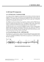
3. TECHNICAL BRIEF In the GSM receive path, the received RF signals are applied through their bandpass filters and downconverted directly to baseband in the RTR6235 transceiver IC. These baseband outputs are routed to the ESM IC for further signal processing. The GSM/EDGE transmit path employs one stage of up-conversion and, in order to improve efficiency, is divided into phase and amplitude components to produce an open-loop Polar topology: 1. The on-chip quadrature up-converter translates the GMSK-modulated signal or 8- PSK modulated signal, to a constant envelope phase signal at RF; 2. The amplitude-modulated (AM) component is applied to the ramping control pin of Polar power amplifier from a DAC within the ESM KE990/KE990c power supply voltages are managed and regulated by the PM6635 Power Management IC. This versatile device integrates all wireless handset power management, general housekeeping, and user interface support functions into a single mixed signal IC. It monitors and controls the external power source and coordinates battery recharging while maintaining the handset supply voltages using low dropout, programmable regulators. The device's general housekeeping functions include an ADC and analog multiplexer circuit for monitoring on-chip voltage sources, charging status, and current flow, as well as user-defined off-chip variables such as temperature, RF output power, and battery ID. Various oscillator, clock, and counter circuits support IC and higher-level handset functions. Key parameters such as under-voltage lockout and crystal oscillator signal presence are monitored to protect against detrimental conditions. LGE Internal Use Only - 16 - Copyright © 2008 LG Electronics. Inc. All right reserved. Only for training and service purposes
-
 1
1 -
2
-
3
-
4
-
5
-
6
-
7
-
8
-
9
-
 10
10 -
 11
11 -
 12
12 -
 13
13 -
 14
14 -
 15
15 -
 16
16 -
 17
17 -
 18
18 -
 19
19 -
 20
20 -
21
-
22
-
23
-
24
-
25
-
26
-
27
-
28
-
29
-
30
-
31
-
32
-
33
-
34
-
35
-
36
-
37
-
38
-
39
-
40
-
41
-
42
-
43
-
44
-
45
-
46
-
47
-
48
-
49
-
50
-
51
-
52
-
53
-
54
-
55
-
56
-
57
-
58
-
59
-
60
-
61
-
62
-
63
-
64
-
65
-
66
-
67
-
68
-
69
-
70
-
71
-
72
-
73
-
74
-
75
-
76
-
77
-
78
-
79
-
80
-
81
-
82
-
83
-
84
-
85
-
86
-
87
-
88
-
89
-
90
-
91
-
92
-
93
-
94
-
95
-
96
-
97
-
98
-
99
-
100
-
101
-
102
-
103
-
104
-
105
-
106
-
107
-
108
-
109
-
110
-
111
-
112
-
113
-
114
-
115
-
116
-
117
-
118
-
119
-
120
-
121
-
122
-
123
-
124
-
125
-
126
-
127
-
128
-
129
-
130
-
131
-
132
-
133
-
134
-
135
-
136
-
137
-
138
-
139
-
140
-
141
-
142
-
143
-
144
-
145
-
146
-
147
-
148
-
149
-
150
-
151
-
152
-
153
-
154
-
155
-
156
-
157
-
158
-
159
-
160
-
161
-
162
-
163
-
164
-
165
-
166
-
167
-
168
-
169
-
170
-
171
-
172
-
173
-
174
-
175
-
176
-
177
-
178
-
179
-
180
-
181
-
182
-
183
-
184
-
185
-
186
-
187
-
188
-
189
-
190
-
191
-
192
-
193
-
194
-
195
-
196
-
197
-
198
-
199
-
200
-
201
-
202
-
203
-
204
 |
 |
