MSI P31 NEO-F User Guide - Page 54
DRAM RAS# Activate to Prechar
 |
UPC - 816909040975
View all MSI P31 NEO-F manuals
Add to My Manuals
Save this manual to your list of manuals |
Page 54 highlights
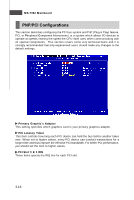
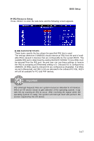
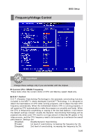
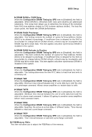
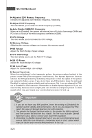
BIOS Setup DRAM RAS# to CAS# Delay W hen the Configuration DRAM Timing by SPD sets to [Disabled], the field is adjustable. W hen DRAM is refreshed, both rows and columns are addressed separately. This setup item allows you to determine the timing of the transition from RAS (row address strobe) to CAS (column address strobe). The less the clock cycles, the faster the DRAM performance. DRAM RAS# Precharge W hen the Configuration DRAM Timing by SPD sets to [Disabled], this field is adjustable. This setting controls the number of cycles for Row Address Strobe (RAS) to be allowed to precharge. If insufficient time is allowed for the RAS to accumulate its charge before DRAM refresh, refresh may be incomplete and DRAM may fail to retain data. This item applies only when synchronous DRAM is installed in the system. DRAM RAS# Activate to Prechar W hen the Configuration DRAM Timing by SPD sets to [Disabled], this field is adjustable. This item controls the number of cycles for Row Address Strobe (RAS) to be allowed to precharge. If insufficient time is allowed for the RAS to accumulate its charge before DRAM refresh, refresh may be incomplete and DRAM may fail to retain data. This item applies only when synchronous DRAM is installed in the system. DRAM TRFC W hen the Configuration DRAM Timing by SPD sets to [Disabled], the field is adjustable. This setting determines the time RFC takes to read from and write to a memory cell. DRAM TWR W hen the Configuration DRAM Timing by SPD sets to [Disabled], the field is adjustable. Minimum time interval between end of write data burst and the start of a precharge command. Allows sense amplifiers to restore data to cells. DRAM TWTR W hen the Configuration DRAM Timing by SPD sets to [Disabled], the field is adjustable. Minimum time interval between the end of write data burst and the start of a column-read command. It allows I/O gating to overdrive sense amplifiers before read command starts. DRAM TRRD W hen the Configuration DRAM Timing by SPD sets to [Disabled], the field is adjustable. Specifies the active-to-active delay of different banks. Time interval between a read and a precharge command. DRAM TRTP W hen the Configuration DRAM Timing by SPD sets to [Disabled], the field is adjustable. Time interval between a read and a precharge command. FSB/Memory Ratio This item will allow you to adjust the FSB/Ratio of the memory. 3-21
-
 1
1 -
2
-
3
-
4
-
5
-
6
-
7
-
8
-
9
-
10
-
11
-
12
-
13
-
14
-
15
-
16
-
17
-
18
-
19
-
20
-
21
-
22
-
23
-
24
-
25
-
26
-
27
-
28
-
29
-
30
-
31
-
32
-
33
-
34
-
35
-
36
-
37
-
38
-
39
-
40
-
41
-
42
-
43
-
44
-
45
-
46
-
47
-
48
-
 49
49 -
 50
50 -
 51
51 -
 52
52 -
 53
53 -
 54
54 -
 55
55 -
 56
56 -
 57
57 -
 58
58 -
 59
59 -
60
-
61
-
62
-
63
-
64
-
65
-
66
-
67
-
68
-
69
-
70
-
71
-
72
-
73
-
74
-
75
-
76
-
77
-
78
-
79
-
80
-
81
-
82
-
83
-
84
-
85
-
86
-
87
-
88
-
89
-
90
 |
 |
