MSI P35 User Guide - Page 60
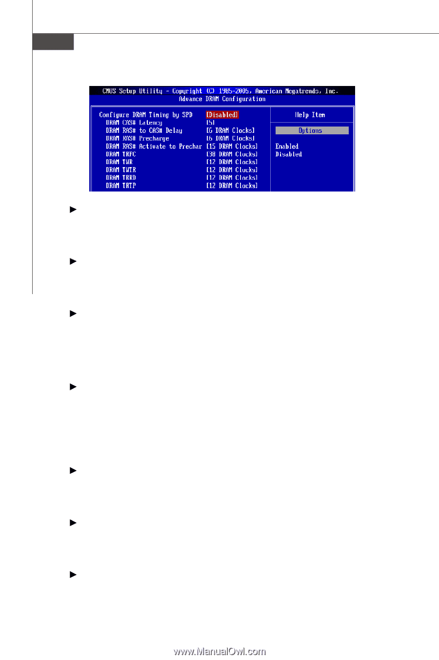
MS-7345 Mainboard, Configuration DRAM Timing by SPD, DRAM CAS# Latency, DRAM RAS# Precharge, DRAM
 |
View all MSI P35 manuals
Add to My Manuals
Save this manual to your list of manuals |
Page 60 highlights
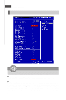
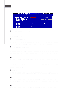
MS-7345 Mainboard Configuration DRAM Timing by SPD Setting to [Enabled] enables DRAM CAS# Latency automatically to be determined by BIOS based on the configurations on the SPD (Serial Presence Detect) EEPROM on the DRAM module. DRAM CAS# Latency W hen the Configuration DRAM Timing by SPD sets to [Disabled], the field is adjustable.This controls the CAS latency, which determines the timing delay (in clock cycles) before SDRAM starts a read command after receiving it. DRAM RAS# to CAS# Delay W hen the Configuration DRAM Timing by SPD sets to [Disabled], the field is adjustable. W hen DRAM is refreshed, both rows and columns are addressed separately. This setup item allows you to determine the timing of the transition from RAS (row address strobe) to CAS (column address strobe). The less the clock cycles, the faster the DRAM performance. DRAM RAS# Precharge W hen the Configuration DRAM Timing by SPD sets to [Disabled], this field is adjustable. This setting controls the number of cycles for Row Address Strobe (RAS) to be allowed to precharge. If insufficient time is allowed for the RAS to accumulate its charge before DRAM refresh, refresh may be incomplete and DRAM may fail to retain data. This item applies only when synchronous DRAM is installed in the system. DRAM TRFC W hen the Configuration DRAM Timing by SPD sets to [Disabled], the field is adjustable. This setting determines the time RFC takes to read from and write to a memory cell. DRAM TWR W hen the Configuration DRAM Timing by SPD sets to [Disabled], the field is adjustable. Minimum time interval between end of write data burst and the start of a precharge command. Allows sense amplifiers to restore data to cells. DRAM TWTR W hen the Configuration DRAM Timing by SPD sets to [Disabled], the field is adjustable. Minimum time interval between the end of write data burst and the 3-22
-
 1
1 -
2
-
3
-
4
-
5
-
6
-
7
-
8
-
9
-
10
-
11
-
12
-
13
-
14
-
15
-
16
-
17
-
18
-
19
-
20
-
21
-
22
-
23
-
24
-
25
-
26
-
27
-
28
-
29
-
30
-
31
-
32
-
33
-
34
-
35
-
36
-
37
-
38
-
39
-
40
-
41
-
42
-
43
-
44
-
45
-
46
-
47
-
48
-
49
-
50
-
51
-
52
-
53
-
54
-
 55
55 -
 56
56 -
 57
57 -
 58
58 -
 59
59 -
 60
60 -
 61
61 -
 62
62 -
 63
63 -
 64
64 -
 65
65 -
66
-
67
-
68
-
69
-
70
-
71
-
72
-
73
-
74
-
75
-
76
-
77
-
78
-
79
-
80
-
81
-
82
-
83
-
84
-
85
-
86
-
87
-
88
-
89
-
90
-
91
-
92
-
93
-
94
-
95
-
96
-
97
-
98
-
99
-
100
-
101
-
102
-
103
-
104
-
105
-
106
-
107
-
108
-
109
-
110
-
111
-
112
-
113
-
114
-
115
-
116
-
117
-
118
-
119
-
120
-
121
 |
 |