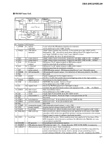
Pioneer DEH-340 Service Manual - Page 22
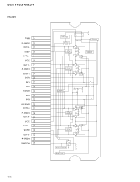
Pin FunctionsTC9495F2 - deh 3400 clock
 |
View all Pioneer DEH-340 manuals
Add to My Manuals
Save this manual to your list of manuals |
Page 22 highlights
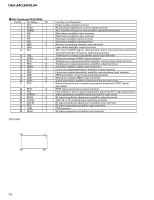
DEH-340,3400,34 - Pin Functions(TC9495F2) Pin No. Pin Name I/O 1 TESTO 2 hso O 3 uhso O 4 EMPH O 5 LRCK O 6 VSS 7 BCK O 8 AOUT O 9 DOUT O 10 MBOV O 11 IPF O 12 SBOK O 13 CLCK I/O 14 VDD 15 VSS 16 DATA O 17 SFSY O 18 SBSY O 19 SPCK O 20 SPDA O 21 COFS O 22 MONIT O 23 VDD 24 TESIO0 I 25 P2VREF 26 HSSW O 27 ZDET O 28 PDO O 29 TMAXS O 30 TAMX O 31 LPFN I 32 LPFO O 33 PVREF 34 VCOREF I 35 VCOF O 36 AVSS 37 SLCO O 38 RFI I 39 AVDD 40 RFCT I 41 RFZI I 42 RFRP I 43 FEI I 44 SBAD I 45 TSIN I 46 TEI I 47 TEZI I 48 FOO O 49 TRO O 50 VREF 51 RFGC O 52 TEBC O 53 FMO O 54 FVO O 55 DMO O 56 2VREF 57 SEL O Function and Operation Test mode terminal Replay speed flag output terminal Replay speed flag output terminal Emphasis flag output terminal for sub code Q data Channel clock (44.1 kHz) output terminal Digital ground terminal Bit clock output terminal Digital audio data output terminal Digital out output terminal Buffer memory over signal output terminal Correction flag output terminal CRCC decision result output for sub code Q data Clock input/output terminal for sub code P-W data read Digital + power supply terminal (5 V) Digital ground terminal Sub code P-W data output terminal Replay-system frame sync signal output terminal Sub code block sync output terminal Clock for processor status signal read Processor status signal output terminal Correction-system frame clock (7.35 kHz) output terminal LSI internal signal output terminal Digital + power supply terminal (5 V) Test input/output terminal PLL-system only 2VREF terminal The VREF voltage is reached for double or quad speed. One-bit DAC zero detection flag output terminal Phase error signal issue between the EFM and PLCK signals TMAX detection result output terminal TMAX detection result output terminal Reverse input terminal of amplifier for lowpass filter Output terminal of amplifier for lowpass filter PLL-system only VREF terminal VCO center frequency reference level terminal Filter terminal for VCO Analog-system ground terminal Output terminal of DAC for data slice level generation RF signal input terminal Analog-system power supply terminal (5 V) RFRP signal center level input terminal Input terminal for RFRP signal zero cross RF ripple signal input terminal Focus error signal input terminal Sub beam addition signal input terminal Test input terminal Tracking error input terminal Input terminal for tracking error or zero cross Focus equalizer output terminal Tracking equalizer output terminal Analog reference power supply terminal RF amplitude adjustment control signal output terminal Tracking balance control signal output terminal Feed equalizer output terminal Speed error signal or feed search EQ output Disc equalizer output terminal Analog reference power supply terminal APC circuit ON/OFF signal output terminal 53
-
 1
1 -
2
-
3
-
4
-
5
-
6
-
7
-
8
-
9
-
10
-
11
-
12
-
13
-
14
-
15
-
16
-
 17
17 -
 18
18 -
 19
19 -
 20
20 -
 21
21 -
 22
22 -
 23
23 -
 24
24 -
 25
25 -
 26
26 -
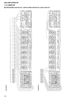 27
27 -
28
-
29
-
30
-
31
-
32
-
33
-
34
-
35
-
36
-
37
 |
 |
