Pioneer DV-606D Service Manual - Page 14
Pcb Connection Diagram
 |
View all Pioneer DV-606D manuals
Add to My Manuals
Save this manual to your list of manuals |
Page 14 highlights
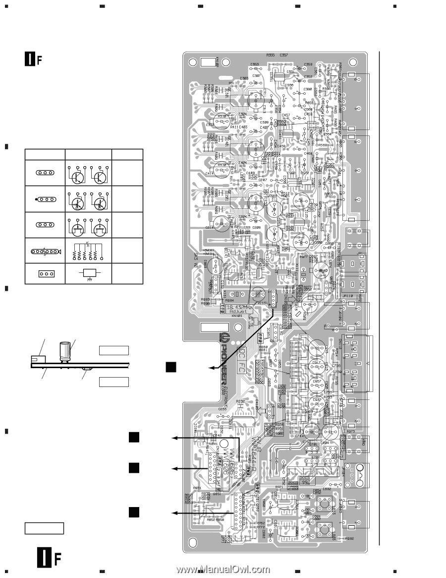
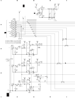
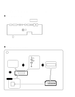
1 2 3 DV-606D 3. PCB CONNECTION DIAGRAM AVJB ASSY A NOTE FOR PCB DIAGRAMS : 1. Part numbers in PCB diagrams match those in the schematic diagrams. 2. A comparison between the main parts of PCB and schematic diagrams is shown below. Symbol In PCB Diagrams Symbol In Schematic Diagrams B C EB C E Part Name BCE Transistor BCE B C EB C E Transistor with resistor B D G SD G S Field effect DGS transistor Resistor array 3-terminal regulator 3. The parts mounted on this PCB include all necessary parts for several destinations. For further information for respective destinations, be sure to check with the schematic diagram. 4. View point of PCB diagrams. Connector Capacitor SIDE A C P.C.Board Chip Part SIDE B H CN801 H CN804 H CN803 D SIDE A H CN802 (VNP1644-A) 14 1 2 3 4 Q354 IC351 Q356 IC301 Q454 Q453 IC451 Q554 IC401 Q553 IC501 IC551 Q254 IC201 Q501 IC251 Q253 Q502 IC171 IC141 IC121 IC151 IC131 IC111 Q871 IC881 VC131 IC851 Q911 -Q913 Q951 -Q954 Q933 Q932 Q753 Q901 IC231 Q931 IC231 Q701 Q801 Q702 Q802 Q804 Q805 Q807 Q808 Q761 IC651 Q762 Q853 Q852 IC601 Q771 Q772 4
-
 1
1 -
2
-
3
-
4
-
5
-
6
-
7
-
8
-
 9
9 -
 10
10 -
 11
11 -
 12
12 -
 13
13 -
 14
14 -
 15
15 -
 16
16 -
 17
17
 |
 |