Pioneer DV-606D Service Manual - Page 17

Ic Information

Page 17 highlights

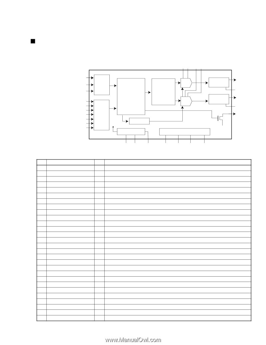
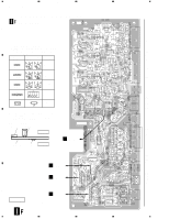
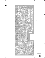
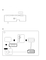
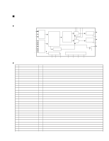
DV-606D 5. IC INFORMATION • The information shown in the list is basic information and may not correspond exactly to that shown in the schematic diagrams. PCM1716E (AVJB ASSY : IC201,IC301 and IC401) • DAC VCC2L AGND2L VCC2R AGND2R ÷ Block Diagram BCKIN LRCIN DIN ML/IIS MC/DM1 MD/DM0 CS/IWO MODE MUTE RST Serial Input 8X I / F Oversampling Digital Filter with Function Mode Controller Control I / F SCK BPZ-Cont. Multi-Level Delta-Signal Modulator DAC DAC Low-pass Filter Low-pass Filter Open Drain Crystal OSC Power Supply VOUTL EXTL VOUTR EXTR ZERO XTI XTO CLKO VCC1 AGND1 VDD DGND ÷ Pin Function No. Pin Name I/O Function 1 LRCIN IN Left & right Clock Input. This clock is equal tothe sampling rate-fs. *1 2 DIN IN Serial Audio DATA Input 3 BCKIN IN Bit Clock Input for Serial Audio DATA 4 CLKO OUT Buffered Output of Oscillator. Equivalent to System Clock. 5 XT1 IN Oscillator Input (External Clock Input) 6 XTO OUT Oscillator Output 7 DGND - Digital Grand 8 VDD - Digital Power +5V 9 VCC2R - Analog Power +5V 10 AGND2R - Analog Grand 11 EXTR OUT R-ch, Common Pin of Analog Output Amp 12 NC - Non Connection 13 VOUTR OUT R-ch Analog Voltage Output of Audio Signal 14 AGND1 - Analog Grand 15 VCC1 - Analog Power +5V 16 VOUTL OUT L-ch Analog Voltage Output of Audio Signal 17 NC - Non Connection 18 EXTL OUT L-ch, Common Pin of Analog Output Amp 19 AGND2L - Analog Grand 20 VCC2L - Analog Power +5V 21 ZERO OUT Zero Data Flag 22 RESET IN Reset. When this pin is low,the DF & Modulator are held in reset. *2 23 CS/IWO IN Chip Select/Input Format Selection. When this pin is low, the Mode Control is effective. *3 24 MODE IN Mode Control Select (H:Software, L:Hardware) *2 25 MUTE IN Mute Control *2 26 MD/DM0 IN Mode Control, Data/De-emphasis selection 1 *2 27 MC/DM1 IN Mode Control, BCK/De-emphasis selection 1 *2 28 ML/IIS IN Mode Control, WDCK/Input format selection 1 *2 *1 : Schmit Trigger input *2 : Schmit Trigger input with pull-up resister *3 : Schmit Trigger input with pull-down resister 17

  • 1
  • 2
  • 3
  • 4
  • 5
  • 6
  • 7
  • 8
  • 9
  • 10
  • 11
  • 12
  • 13
  • 14
  • 15
  • 16
  • 17

17
DV-606D
÷
Block Diagram
• The information shown in the list is basic information and may not correspond exactly to that shown in the schematic diagrams.
PCM1716E (AVJB ASSY : IC201,IC301 and IC401)
5. IC INFORMATION
.
o
N
e
m
a
N
n
i
P
O
/
I
n
o
i
t
c
n
u
F
1
N
I
C
R
L
N
I
1
*
.
s
f
-
e
t
a
r
g
n
i
l
p
m
a
s
e
h
t
o
t
l
a
u
q
e
s
i
k
c
o
l
c
s
i
h
T
.
t
u
p
n
I
k
c
o
l
C
t
h
g
i
r
&
t
f
e
L
2
N
I
D
N
I
t
u
p
n
I
A
T
A
D
o
i
d
u
A
l
a
i
r
e
S
3
N
I
K
C
B
N
I
A
T
A
D
o
i
d
u
A
l
a
i
r
e
S
r
o
f
t
u
p
n
I
k
c
o
l
C
t
i
B
4
O
K
L
C
T
U
O
.
k
c
o
l
C
m
e
t
s
y
S
o
t
t
n
e
l
a
v
i
u
q
E
.
r
o
t
a
l
l
i
c
s
O
f
o
t
u
p
t
u
O
d
e
r
e
f
f
u
B
5
1
T
X
N
I
)
t
u
p
n
I
k
c
o
l
C
l
a
n
r
e
t
x
E
(
t
u
p
n
I
r
o
t
a
l
l
i
c
s
O
6
O
T
X
T
U
O
t
u
p
t
u
O
r
o
t
a
l
l
i
c
s
O
7
D
N
G
D
-
d
n
a
r
G
l
a
t
i
g
i
D
8
D
D
V
-
V
5
+
r
e
w
o
P
l
a
t
i
g
i
D
9
R
2
C
C
V
-
V
5
+
r
e
w
o
P
g
o
l
a
n
A
0
1
R
2
D
N
G
A
-
d
n
a
r
G
g
o
l
a
n
A
1
1
R
T
X
E
T
U
O
p
m
A
t
u
p
t
u
O
g
o
l
a
n
A
f
o
n
i
P
n
o
m
m
o
C
,
h
c
-
R
2
1
C
N
-
n
o
i
t
c
e
n
n
o
C
n
o
N
3
1
R
T
U
O
V
T
U
O
l
a
n
g
i
S
o
i
d
u
A
f
o
t
u
p
t
u
O
e
g
a
t
l
o
V
g
o
l
a
n
A
h
c
-
R
4
1
1
D
N
G
A
-
d
n
a
r
G
g
o
l
a
n
A
5
1
1
C
C
V
-
V
5
+
r
e
w
o
P
g
o
l
a
n
A
6
1
L
T
U
O
V
T
U
O
l
a
n
g
i
S
o
i
d
u
A
f
o
t
u
p
t
u
O
e
g
a
t
l
o
V
g
o
l
a
n
A
h
c
-
L
7
1
C
N
-
n
o
i
t
c
e
n
n
o
C
n
o
N
8
1
L
T
X
E
T
U
O
p
m
A
t
u
p
t
u
O
g
o
l
a
n
A
f
o
n
i
P
n
o
m
m
o
C
,
h
c
-
L
9
1
L
2
D
N
G
A
-
d
n
a
r
G
g
o
l
a
n
A
0
2
L
2
C
C
V
-
V
5
+
r
e
w
o
P
g
o
l
a
n
A
1
2
O
R
E
Z
T
U
O
g
a
l
F
a
t
a
D
o
r
e
Z
2
2
T
E
S
E
R
N
I
2
*
.
t
e
s
e
r
n
i
d
l
e
h
e
r
a
r
o
t
a
l
u
d
o
M
&
F
D
e
h
t
,
w
o
l
s
i
n
i
p
s
i
h
t
n
e
h
W
.
t
e
s
e
R
3
2
O
W
I
/
S
C
N
I
3
*
.
e
v
i
t
c
e
f
f
e
s
i
l
o
r
t
n
o
C
e
d
o
M
e
h
t
,
w
o
l
s
i
n
i
p
s
i
h
t
n
e
h
W
.
n
o
i
t
c
e
l
e
S
t
a
m
r
o
F
t
u
p
n
I
/
t
c
e
l
e
S
p
i
h
C
4
2
E
D
O
M
N
I
2
*
)
e
r
a
w
d
r
a
H
:
L
,
e
r
a
w
t
f
o
S
:
H
(
t
c
e
l
e
S
l
o
r
t
n
o
C
e
d
o
M
5
2
E
T
U
M
N
I
2
*
l
o
r
t
n
o
C
e
t
u
M
6
2
0
M
D
/
D
M
N
I
2
*
1
n
o
i
t
c
e
l
e
s
s
i
s
a
h
p
m
e
-
e
D
/
a
t
a
D
,
l
o
r
t
n
o
C
e
d
o
M
7
2
1
M
D
/
C
M
N
I
2
*
1
n
o
i
t
c
e
l
e
s
s
i
s
a
h
p
m
e
-
e
D
/
K
C
B
,
l
o
r
t
n
o
C
e
d
o
M
8
2
S
I
I
/
L
M
N
I
2
*
1
n
o
i
t
c
e
l
e
s
t
a
m
r
o
f
t
u
p
n
I
/
K
C
D
W
,
l
o
r
t
n
o
C
e
d
o
M
÷
Pin Function
*1 : Schmit Trigger input
*2 : Schmit Trigger input with pull-up resister
*3 : Schmit Trigger input with pull-down resister
Serial
Input
I / F
8X
Oversampling
Digital Filter
with
Function
Controller
Multi-Level
Delta-Signal
Modulator
DAC
DAC
Low-pass
Filter
Low-pass
Filter
VOUTL
EXTL
VOUTR
EXTR
ZERO
DGND
VDD
AGND1
VCC1
CLKO
XTO
XTI
BCKIN
LRCIN
DIN
ML/IIS
MC/DM1
MD/DM0
CS/IWO
MODE
MUTE
RST
VCC2L
AGND2L
VCC2R
AGND2R
Mode
Control
I / F
BPZ-Cont.
Crystal OSC
Power Supply
Open Drain
SCK
• DAC