Pioneer VSX-D509S Service Manual - Page 53
W24257aj-12 D.d & Input Assy : Ic1301, Tc9273f-007 D.d & Input Assy : Ic101
 |
View all Pioneer VSX-D509S manuals
Add to My Manuals
Save this manual to your list of manuals |
Page 53 highlights
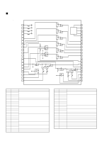
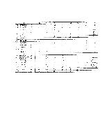
VSX-D509S W24257AJ-12 (D.D & INPUT ASSY : IC1301) • 32K × 8 High-Speed CMOS Static RAM • Block Diagram • Pin Function VDD 28 DSS 14 A0 10 A14 1 DECORER CS 20 OE 22 WE 27 CONTROL CORE ARRAY DATA I/O 11 I/O1 19 I/O8 No. Pin Name Function 1 A14 2 A12 3 A7 4 A6 5 A5 6 A4 7 A3 8 A2 Addres Inputs 9 A1 10 A0 21 A10 23 A11 24 A9 25 A8 26 A13 11 I/O1 12 I/O2 13 I/O3 15 16 I/O4 I/O5 Data Inputs/Outputs 17 I/O6 18 I/O7 19 I/O8 14 Vss Ground 20 CS Chip Select Input 22 OE Output Enable Input 27 WE Write Enable Input 28 Vdd Power Supply TC9273F-007 (D.D & INPUT ASSY : IC101) • Analog Switch Array • Block Diagram DSS VDD 1 28 S1 2 S2 3 S3 4 S4 5 S5 6 S6 7 S7 8 S8 9 S9 10 S10 11 S11 12 (L-ch) 10 bit Latch Circuit (R-ch) 10 bit Latch Circuit 27 S1 26 S2 25 S3 24 S4 23 S5 22 S6 21 S7 20 S8 19 S9 18 S10 17 S11 • Pin Function No. 1 2, 27 3, 26 4, 25 5, 24 6, 23 7, 22 8, 21 9, 20 10, 19 21, 18 26, 17 13 14 15 16 28 Pin Name VSS S1 S2 S3 S4 S5 S6 S7 S8 S9 S10 S11 GND CK DATA STB VDD Function Minus Power Supply Input and Output Digital Ground Clock Input Data Input Strobe Input Plus Power Supply Level Shift + Shift Register Circuit 13 14 GND CK 15 16 DATA STB 53
-
 1
1 -
2
-
3
-
4
-
5
-
6
-
7
-
8
-
9
-
10
-
11
-
12
-
13
-
14
-
15
-
16
-
17
-
18
-
19
-
20
-
21
-
22
-
23
-
24
-
25
-
26
-
27
-
28
-
29
-
30
-
31
-
32
-
33
-
34
-
35
-
36
-
37
-
38
-
39
-
40
-
41
-
42
-
43
-
44
-
45
-
46
-
47
-
 48
48 -
 49
49 -
 50
50 -
 51
51 -
 52
52 -
 53
53 -
 54
54 -
 55
55 -
 56
56 -
 57
57 -
 58
58 -
59
-
60
-
61
 |
 |
