Pioneer VSX-D906S Service Manual - Page 49
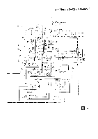
L9 tg - schematic
 |
View all Pioneer VSX-D906S manuals
Add to My Manuals
Save this manual to your list of manuals |
Page 49 highlights
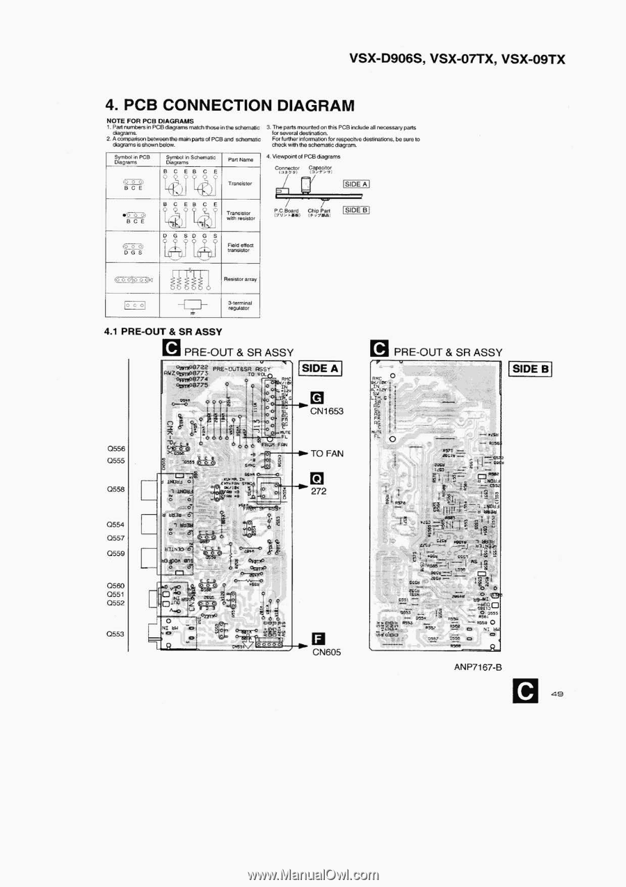
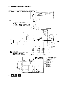
VSX-D906S, VSX-07TX, VSX-09TX 4. PCB CONNECTION DIAGRAM MOTE FOR PCB DIAGRAMS 1. Part numbers in PCB diagrams match those in the schematic diagrams. 2. A compar i son bet ween th main parle of PCB and schematic diagrams is shown below. 3. The pans mounted on this PCB include all necessary parts for several destination. For further information for respecitve destinations, be sure to check with the schematic diagram. Symbol in PCB Diagrams Symbol in Schematic Diagrams Psrt Name 4. Viewpoint of PCB diagrams Connector Capacitor !Ga s t'l Il G Cl) BCE Transistor SIDE A ~ '0 0 0 ) BCE I ~G o 0 ' DG S < QJ! Transistor with resistor L9 tg Field ef/ect transistor P .C.Board Chip Part (Toute ets l ( 3 / T e al ~S IDE B ~ 0 0 0 ~0 0 G Resistor array 0 00 3-terminal regulator 4.1 PRE-OUT & SR ASSY Q556 Q555 Q558 Q554 Q557 Q559 PRE-O UT 82 SR ASSY . RBRF 8 72 2 PRE 'CDTSSR F!SST RIIZ Obsttf58 7 7 6 / . .TD VOL l o ssftfoB7 7 4 0 . OgyttfoB7 76 RMC / le 0 ItNa v Pig ..i g) JK,P SR '0 r S L RG . FR !Ltc TOTE FL 5, . t b O RRGKR F SIDE A CN1653 TO FAN J S NDtht ',0 " l '' 0,- ! O '. ~ ' ..«" ' r.iKmii Nt rSe.s1 N elR/ !sBK B rse wr 272 cl ucl31!- :0 Kr 1s b-/-" ii ttgl NSO.'O II PRE-O UT 8L SR ASSY R MC 0 SK/ i SK lIl. Ntav 'I LI M. G 'I SIDE B Nv Tr. Fi. BBCIV e!N a r , g „,l ' =
-
 1
1 -
2
-
3
-
4
-
5
-
6
-
7
-
8
-
9
-
10
-
11
-
12
-
13
-
14
-
15
-
16
-
17
-
18
-
19
-
20
-
21
-
22
-
23
-
24
-
25
-
26
-
27
-
28
-
29
-
30
-
31
-
32
-
33
-
34
-
35
-
36
-
37
-
38
-
39
-
40
-
41
-
42
-
43
-
 44
44 -
 45
45 -
 46
46 -
 47
47 -
 48
48 -
 49
49 -
 50
50 -
 51
51 -
 52
52 -
 53
53 -
 54
54 -
55
-
56
-
57
-
58
-
59
-
60
-
61
-
62
-
63
-
64
-
65
-
66
-
67
-
68
-
69
-
70
-
71
-
72
-
73
-
74
-
75
-
76
-
77
-
78
-
79
-
80
-
81
-
82
-
83
-
84
 |
 |