Pioneer VSX-D906S Service Manual - Page 69
C output enable signal for M663 I H: Enabled.
 |
View all Pioneer VSX-D906S manuals
Add to My Manuals
Save this manual to your list of manuals |
Page 69 highlights
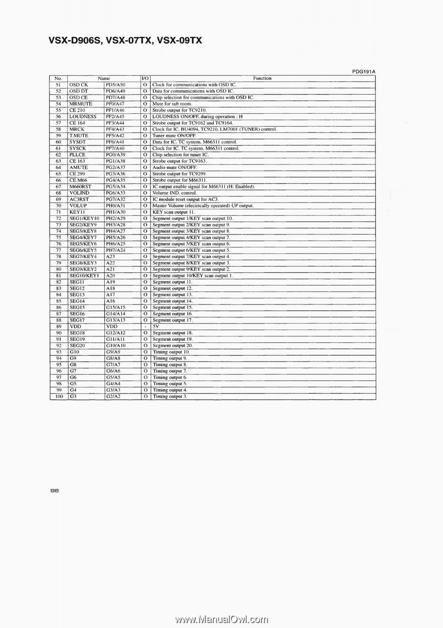
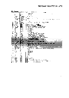
VSX-O906S, VSX-07TX, VSX-09TX No Name 51 OSD CK PD5/A 50 57 OSD DT PD6/A49 OSD CE PD7/A48 54 MR M UT E PFO/A47 55 CE 210 PF I/A46 LOUDNESS PF2/A45 57 CE 164 PF3/A44 . 8 MRCK PF4/A43 59 T.M UT E PF5/A42 60 SYSDT P F6/A4 1 6 1 SYSCK PF7/A40 62 PLLCE PGO/A39 CE )63 PG I /A38 64 A M UT E PG2/A37 CE 299 PG3/A36 66 CE M66 PG4/A35 67 M660RST PG5/A34 VOLIND PG6/A33 69 AC3RST P G7/A 32 70 VOL UP PHO/A31 7 1 KEY I ) PH I/A30 72 S EG)/K E Y ) 0 PH2/A29 73 S EG2/KEY 9 PH3/A28 74 S EG3/KE Y 8 PH4/A27 75 S EG4/KEY 7 PH 5/A26 76 S EG5/KEY 6 PH6/A 2S 77 S EG6/KEY S PH7/A24 78 S EG7/KEY 4 A23 79 S EG8/KE Y 3 A 2 7 80 S EG9/KEY 2 A 2 1 81 S EG)0/KEY ) A20 82 SEG I I A)9 83 SEG12 A)8 84 SEG I 3 A17 85 SEG14 A)6 86 SEG15 G15/A 15 87 SEG16 G14/A 14 SEG17 G)3/A 13 VDD VDD 90 SEG18 GI2/A 12 9 1 SEG19 9'7 SEG20 G I I/A I I G I 0/A 10 93 G I 0 G9/A9 94 G9 G 8/A 8 95 G8 G7/A7 96 G7 G6/A6 97 G6 G 5/A 5 G4/A4 99 G3/A3 100 G3 G2/A2 I/O Function 0 Clock for communications with OSD IC. 0 Data for communications with OSD IC. Chip selection for communications with OSD IC . 0 Mute for sub room. 0 Strobe output for TC9210. 0 LOU DNESS ON/OFF, during operation : H Strobe output for TC9162 and TC9164. Clock for IC. BU4094. TC9210. LM7001 (T UNER) control . 0 Tuner mute ON/OFF. 0 Data for IC. TC system. M663) I control. Clock for IC. TC system, M66311 control. 0 Chip selection for tuner IC. Strobe output for TC9163. Audio mute ON/OFF. 0 Strobe output for TC9299. 0 Strobe output for M663 1) . )C output enable signal for M663) I (H: Enabled). 0 Volume IiVD. control. 0 IC module reset output for AC3. 0 Master Volume (electrically operated) UP output. 0 K EY scan output I l . 0 Segment output I/ KEY scan output 10. 0 Segment output 2/KEY scan output 9. 0 Segment output 3/KEY scan output 8. 0 Segment output 4/KEY scan output 7. 0 Segment output S/KEY scan output 6. 0 Segment output 6/KEY scan output 5. 0 Segment output 7/KEY scan output 4. 0 Segment output 8/KEY scan output 3. 0 Segment output 9/KEY scan output 2. 0 S egment output 10/KEY scan output l . 0 Segment output 11. 0 Segment output 12. 0 Segment output 13. 0 Segment output 14. 0 Segment output 15. 0 Segment output 16. 0 Segment output 17. 5V Segment output 18. 0 Segment output 19. 0 Segment output 20. 0 Timing output I O. 0 Timing output 9. Timing output 8. 0 Tinung output 7. 0 Tinung output 6. 0 Timing output 5. 0 Timing output 4. Ttriung output 3. PDG191A 99
-
 1
1 -
2
-
3
-
4
-
5
-
6
-
7
-
8
-
9
-
10
-
11
-
12
-
13
-
14
-
15
-
16
-
17
-
18
-
19
-
20
-
21
-
22
-
23
-
24
-
25
-
26
-
27
-
28
-
29
-
30
-
31
-
32
-
33
-
34
-
35
-
36
-
37
-
38
-
39
-
40
-
41
-
42
-
43
-
44
-
45
-
46
-
47
-
48
-
49
-
50
-
51
-
52
-
53
-
54
-
55
-
56
-
57
-
58
-
59
-
60
-
61
-
62
-
63
-
 64
64 -
 65
65 -
 66
66 -
 67
67 -
 68
68 -
 69
69 -
 70
70 -
 71
71 -
 72
72 -
 73
73 -
 74
74 -
75
-
76
-
77
-
78
-
79
-
80
-
81
-
82
-
83
-
84
 |
 |