Samsung CS-15K5ML Service Manual - Page 9
Samsung CS-15K5ML Manual
 |
View all Samsung CS-15K5ML manuals
Add to My Manuals
Save this manual to your list of manuals |
Page 9 highlights
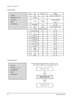
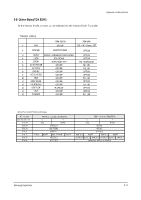
Alignment and Adjustments 2-6 PIN ASSIGNMENT SPECIFICATION PIN NO 1 2 3 4 5 6 7 8 9 10 11 12 13 14 15 16 17 18 19 20 21 22 23 24 25 26 27 28 29 30 31 32 SYMBOL P1.3/T1 P1.6/SCL P1.7/SDA P2.0/TPMW P3.0/ADC0 P3.1/ADC1 P3.2/ADC2 P3.3/ADC3 VSSC/P P0.5 P0.6 VSSA SECPLL VP2 DECDIG PH2LF PH1LF GND3 DECBG EWD VDRB VDRA IFIN1 IFIN2 IREF VSC AGCOUT SIFIN1/DVBIN1 SIFIN2/DVBIN2 GND2 SIFAGC/DVBAGCR REFO/AMOUT/REFIN PIN FUNCTION port 1.3 or Counter/Timer 1 input port 1.6 or IIC-bus clock line port 1.7 or IIC-bus data line port 2.0 or Tuning PWM output port 3.0 or ADC0 input port 3.1 or ADC1 input port 3.2 or ADC2 input port 3.3 or ADC3 input digital ground for m-Controller core and periphery port 0.5(8mA current sinking capability for direct drive of LEDs) port 0.6(8mA current sinking capability for direct drive of LEDs) digital ground of TV-processor SECAM PLL decoupling 2nd supply voltage TV-processor(+8V) supply voltage decoupling of digital circuit of TV-processor phase-2 filter phase-1 filter ground 3 for TV-processor bandgap decoupling East-West drive output vertical drive B output vertical drive A output IF input 1 IF input 2 reference current input vertical sawtooth capacitor tuner AGC output SIF input 1 / DVB input 1 SIF input 2 / DVB input 2 ground 2 for TV processor narrow band PLL filter Automatic Volume Leveling/subcarr reference output/sound IF input/external reference signal input for I signal mixer for DVB operation CHECK VOLTAGE S-By P-On 2-8 Samsung Electronics
-
 1
1 -
2
-
3
-
 4
4 -
 5
5 -
 6
6 -
 7
7 -
 8
8 -
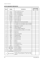 9
9 -
 10
10 -
 11
11 -
 12
12 -
 13
13 -
 14
14 -
15
-
16
-
17
-
18
-
19
-
20
-
21
-
22
-
23
-
24
-
25
-
26
-
27
-
28
-
29
-
30
-
31
-
32
-
33
-
34
-
35
-
36
-
37
-
38
-
39
-
40
-
41
-
42
 |
 |
