SanDisk SDCFRX4-2048-901 Product Manual - Page 21
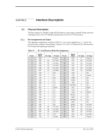
Electrical Description
 |
UPC - 619659028954
View all SanDisk SDCFRX4-2048-901 manuals
Add to My Manuals
Save this manual to your list of manuals |
Page 21 highlights
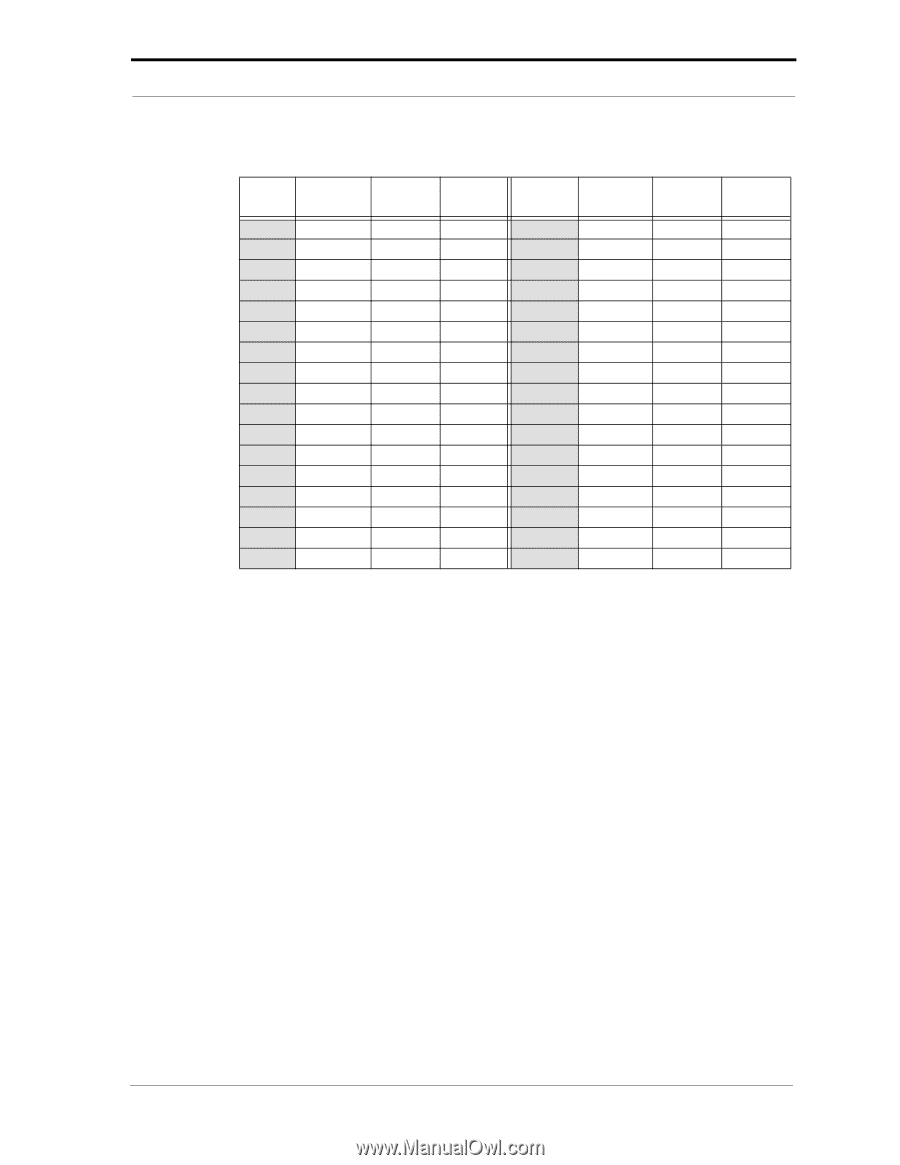
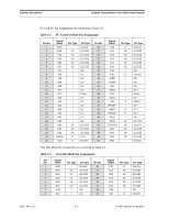
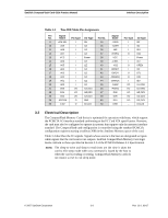
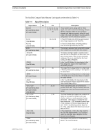
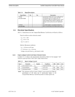
SanDisk CompactFlash Card OEM Product Manual Interface Description Table 3-3 True IDE Mode Pin Assignments Pin Signal No. Name Pin Type I/O Type Pin No. 9 -ATA SEL I I3U 34 10 A09 I I1Z 35 11 A08 I I1Z 36 12 A07 I I1Z 37 13 VCC - Power 38 14 A06 I I1Z 39 15 A05 I I1Z 40 16 A04 I I1Z 41 17 A03 I I1Z 42 18 A02 I I1Z 43 19 A01 I I1Z 44 20 A00 I I1Z 45 21 D00 I/O I1Z,OZ3 46 22 D01 I/O I1Z,OZ3 47 23 D02 I/O I1Z,OZ3 48 24 -IOCS16 O ON3 49 25 -CD2 O Ground 50 Signal Name -IORD -IOWR -WE INTRQ VCC -CSEL -VS2 RESET IORDY -DMARQ -DMACK -DASP -PDIAG D08 D09 D10 GND Pin Type I I I O - I O I O O I I/O I/O I/O I/O I/O - I/O Type I3Z I3Z I3U OZ1 Power I2U OPEN I2Z OT1 OZ1 I3U I1U,ON1 I1U,ON1 I1Z,OZ3 I1Z,OZ3 I1Z,OZ3 Ground 3.2 Electrical Description The CompactFlash Memory Card Series is optimized for operation with hosts, which support the PCMCIA I/O interface standard conforming to the PC Card ATA specification. However, the card may also be configured to operate in systems that support only the memory interface standard. The CompactFlash card configuration is controlled using the standard PCMCIA configuration registers starting at address 200h in the Attribute Memory space of the card. Table 3-4 describes the I/O signals. Signals whose source is the host are designated as inputs while signals that the card sources are outputs. SanDisk CompactFlash Memory Card logic levels conform to those specified in Section 3.3 of the PCMCIA Release 2.1 Specification. NOTE: The sleep-to-write and sleep-to-read times are the time it takes the card to exit sleep mode when any command is issued by the host to when the card is reading or writing. CompactFlash Memory cards do not require a reset to exit sleep mode. © 2007 SanDisk Corporation 3-3 Rev. 12.0, 02/07
-
 1
1 -
2
-
3
-
4
-
5
-
6
-
7
-
8
-
9
-
10
-
11
-
12
-
13
-
14
-
15
-
 16
16 -
 17
17 -
 18
18 -
 19
19 -
 20
20 -
 21
21 -
 22
22 -
 23
23 -
 24
24 -
 25
25 -
 26
26 -
27
-
28
-
29
-
30
-
31
-
32
-
33
-
34
-
35
-
36
-
37
-
38
-
39
-
40
-
41
-
42
-
43
-
44
-
45
-
46
-
47
-
48
-
49
-
50
-
51
-
52
-
53
-
54
-
55
-
56
-
57
-
58
-
59
-
60
-
61
-
62
-
63
-
64
-
65
-
66
-
67
-
68
-
69
-
70
-
71
-
72
-
73
-
74
-
75
-
76
-
77
-
78
-
79
-
80
-
81
-
82
-
83
-
84
-
85
-
86
-
87
-
88
-
89
-
90
-
91
-
92
-
93
-
94
-
95
-
96
-
97
-
98
-
99
-
100
-
101
-
102
-
103
-
104
-
105
-
106
-
107
-
108
 |
 |