SanDisk SDCFX-256-786 Product Manual - Page 31
Table 3-12, Attribute Memory Read Timing Specification, Common and Attribute Memory Read - area
 |
UPC - 619659018795
View all SanDisk SDCFX-256-786 manuals
Add to My Manuals
Save this manual to your list of manuals |
Page 31 highlights
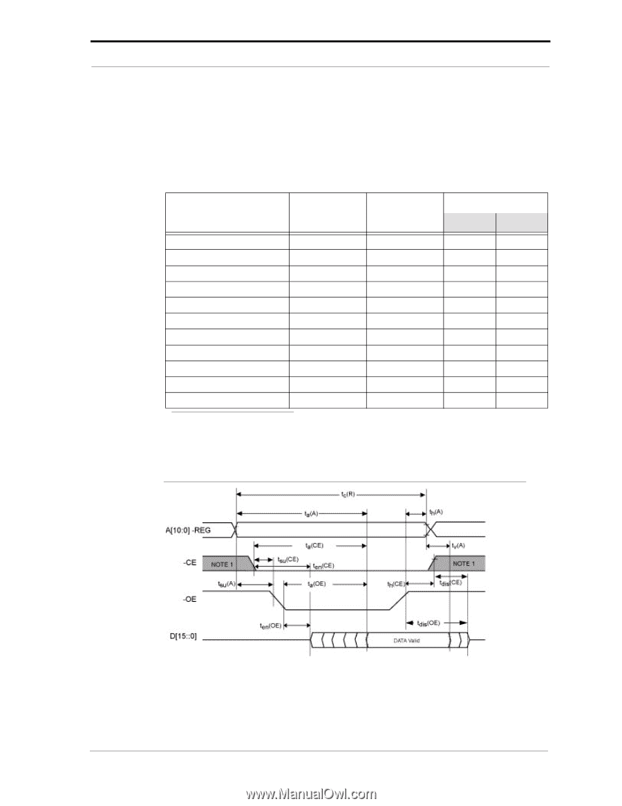
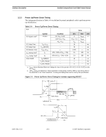
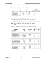
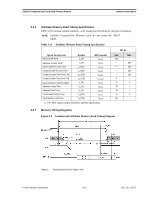
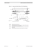
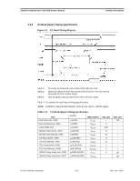
SanDisk CompactFlash Card OEM Product Manual Interface Description 3.3.6 Attribute Memory Read Timing Specification Table 3-12 contains common memory write timing specifications for all types of memory. NOTE: SanDisk CompactFlash Memory cards do not assert the -WAIT signal. Table 3-12 Attribute Memory Read Timing Specification Speed Version Item Read Cycle Time Address Access Timea Card Enable Access Time Output Enable Access Time Output Disable Time from -OE Output Enable Time from -OE Data Valid from Add Changea Address Setup Time Address Hold Time Card Enable Setup Time Card Enable Hold Time Symbol tc (R) ta (A) ta (CE) ta (OE) tdis (OE) ten (OE) tv (A) tsu (A) th (A) tsu(CE) th (CE) IEEE Symbol tAVAV tAVQV tELQV tGLQV tGHQZ tGLQNZ tAXQX tAVGL tGHAX tELGL tGHEH a. The -REG signal timing is identical to address signal timing 300 ns Min. 300 --------- 5 0 30 20 0 20 Max. --300 300 150 100 3.3.7 Memory Timing Diagrams Figure 3-3 Common and Attribute Memory Read Timing Diagram NOTE 1: Shaded areas may be high or low. © 2007 SanDisk Corporation 3-13 Rev. 12.0, 02/07
-
 1
1 -
2
-
3
-
4
-
5
-
6
-
7
-
8
-
9
-
10
-
11
-
12
-
13
-
14
-
15
-
16
-
17
-
18
-
19
-
20
-
21
-
22
-
23
-
24
-
25
-
 26
26 -
 27
27 -
 28
28 -
 29
29 -
 30
30 -
 31
31 -
 32
32 -
 33
33 -
 34
34 -
 35
35 -
 36
36 -
37
-
38
-
39
-
40
-
41
-
42
-
43
-
44
-
45
-
46
-
47
-
48
-
49
-
50
-
51
-
52
-
53
-
54
-
55
-
56
-
57
-
58
-
59
-
60
-
61
-
62
-
63
-
64
-
65
-
66
-
67
-
68
-
69
-
70
-
71
-
72
-
73
-
74
-
75
-
76
-
77
-
78
-
79
-
80
-
81
-
82
-
83
-
84
-
85
-
86
-
87
-
88
-
89
-
90
-
91
-
92
-
93
-
94
-
95
-
96
-
97
-
98
-
99
-
100
-
101
-
102
-
103
-
104
-
105
-
106
-
107
-
108
 |
 |