Sony STR-GX80ES Technical Background - Page 12
MOS FET Thermal Packaging
 |
View all Sony STR-GX80ES manuals
Add to My Manuals
Save this manual to your list of manuals |
Page 12 highlights
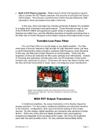
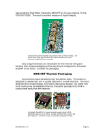
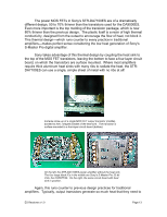
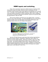
Semiconductor Field Effect Transistors (MOS FETs), four per channel, for the STR-DA7100ES. The result is another measure of signal integrity. A detail of the power amplifier circuit board of the STR-DA7100ES. The twelve black chips are the MOS FET output transistors for three channels (4 MOS FETs per channel). Sony output transistors are remarkable for their internal wiring and bonding, their unique packaging and the way they're configured on the power amplifier circuit board. Consider the packaging. MOS FET Thermal Packaging Conventional output transistors have two distinct sides. The bottom is designed to radiate heat, and is usually attached to a metal heat sink. The top is fashioned from molded plastic, from which heat cannot escape. No matter how much cooling may be available at the top, the plastic package is too thick to conduct heat away from the transistor. On the left, the MOS FET output transistor used in Sony's STRDA9000ES was 2 to 3 mm thick. At right, the MOS FETs used in the DA7100ES is 1 mm thick or less, for far better dissipation of heat. ES Receivers v1.0 Page 12
-
 1
1 -
2
-
3
-
4
-
5
-
6
-
 7
7 -
 8
8 -
 9
9 -
 10
10 -
 11
11 -
 12
12 -
 13
13 -
 14
14 -
 15
15 -
 16
16 -
 17
17 -
18
-
19
-
20
-
21
-
22
-
23
-
24
-
25
-
26
-
27
-
28
-
29
-
30
-
31
-
32
-
33
-
34
-
35
-
36
-
37
-
38
 |
 |
