Sony STR-GX80ES Technical Background - Page 14
Molecular Bonding
 |
View all Sony STR-GX80ES manuals
Add to My Manuals
Save this manual to your list of manuals |
Page 14 highlights
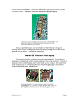
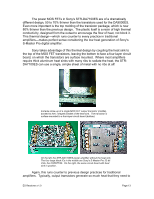
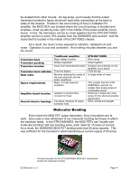
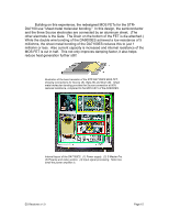
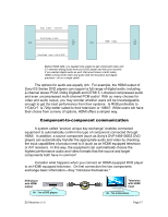
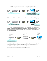
be isolated from other circuits. On big amps, you'll usually find the output transistors bonded to heavy aluminum heat sinks somewhere at the back or sides of the chassis. Thanks to the cool running of Sony's S-Master Pro amplifier, the MOS FETs are located where the circuit topology is shortest and simplest-lined up side-by-side, right in the middle of the power amplifier circuit board. In fact, the transistors can be so close together that the STR-DA7100ES amplifier section is some 70% smaller than the DA9000ES amp section! And the board itself is located in the middle of the DA7100ES chassis. As a result, the music is less exposed to vibration, radiated hum and noise. Operation is cool and consistent. And nothing intrudes between you and the sound. Transistor heat Transistor packing Transistor location Transistor heat radiation Heat sinks Space requirements Amplifier board location Overall chassis topology Traditional amplifier Major design concern Widely separated Away from heat-sensitive parts From the bottom Massive radiating fins made of die cast aluminum (on the better amplifiers) Major, for high powered amplifiers Isolated, to protect other circuits from heat Circuitous, because of output transistor heat STR-DA7100ES Minor issue Close together Surface mount directly on the amplifier circuit board From the top A single sheet of metal 70% smaller than the STRDA9000ES-and far, far smaller than analog amps of comparable power Wherever it makes the most sense for the shortest possible signal paths Short, simple and straight Molecular Bonding Even inside the MOS FET output transistors, Sony innovations are at work. Sony uses a new refinement of our molecular bonding technique to attach the transistor leads. In the STR-DA9000ES, the MOS FETs use "double wire molecular bonding" with two bonding wires, each rated for 15 amps of current. As a result, the DA9000ES MOS FET binding wires had 30 amp capacity. This was sufficient for the transistor's rated instantaneous current supply of 24 amps. The bare transistor for the STR-DA9000ES MOS FET, showing the double wire molecular bonding. ES Receivers v1.0 Page 14
-
 1
1 -
2
-
3
-
4
-
5
-
6
-
7
-
8
-
 9
9 -
 10
10 -
 11
11 -
 12
12 -
 13
13 -
 14
14 -
 15
15 -
 16
16 -
 17
17 -
 18
18 -
 19
19 -
20
-
21
-
22
-
23
-
24
-
25
-
26
-
27
-
28
-
29
-
30
-
31
-
32
-
33
-
34
-
35
-
36
-
37
-
38
 |
 |
