TEAC DW-224E-V Hardware Specification - Page 15
Input/Output Signals
 |
View all TEAC DW-224E-V manuals
Add to My Manuals
Save this manual to your list of manuals |
Page 15 highlights
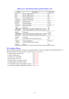
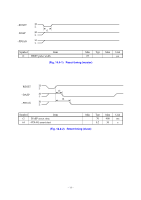
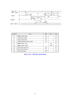
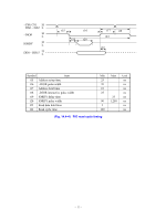
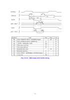
(4) Open-drain output signals ( -IOCS16) • Low level : 0 to 0.4VDC (output sink current 12mA) • Maximum output current at high impedance : ±25µA (5) Input signals (-RESET, -DIOW, -DIOR, -CSEL, -DMACK, DA0 to DA2, -CS0, -CS1) (a) Input signal level • Low level : 0 to 0.8VDC • High level : 2.0 to 5.25VDC • Hysteresis (excluding RESET, -CSEL) : possessed • Maximum input current : ±25µA (excluding the pull-up resistance) • Pull-up resistance -RESET : 10kΩ -CSEL : 47kΩ • Series resistance (-RESET, -DIOW, -DIOR, -DMACK, DA0 to DA2, -CS0, -CS1) : 82Ω 14.3 Input/Output Signals Refer to Table 14.3-1. Among the following signals, the input signal refers to the signal input to the CD-RW drive and the output signal refers to the signal output from the CD-RW drive and the input/output signal refers to the bidirectional signal. (Table 14.3-1) IDE Interface signal summary (Sheet 1 of 2) Signal -CSEL -CS0 -CS1 DD0 DD1 DD2 DD3 DD4 DD5 DD6 DD7 DD8 DD9 DD10 DD11 DD12 DD13 DD14 DD15 -DASP Description Cable select Chip select0 Chip select1 Data bus bit 0 Data bus bit 1 Data bus bit 2 Data bus bit 3 Data bus bit 4 Data bus bit 5 Data bus bit 6 Data bus bit 7 Data bus bit 8 Data bus bit 9 Data bus bit 10 Data bus bit 11 Data bus bit 12 Data bus bit 13 Data bus bit 14 Data bus bit 15 Device active/Slave present Direction IN IN IN IN/OUT IN/OUT IN/OUT IN/OUT IN/OUT IN/OUT IN/OUT IN/OUT IN/OUT IN/OUT IN/OUT IN/OUT IN/OUT IN/OUT IN/OUT IN/OUT IN/OUT - 13 -
-
 1
1 -
2
-
3
-
4
-
5
-
6
-
7
-
8
-
9
-
 10
10 -
 11
11 -
 12
12 -
 13
13 -
 14
14 -
 15
15 -
 16
16 -
 17
17 -
 18
18 -
 19
19 -
 20
20 -
21
-
22
-
23
-
24
-
25
-
26
-
27
-
28
-
29
-
30
-
31
-
32
-
33
-
34
 |
 |