Asus A7S266-VM U2 A7S266-VM/U2 User Manual - Page 47
SDRAM RAS to CAS Delay [4T] - videos
 |
View all Asus A7S266-VM U2 manuals
Add to My Manuals
Save this manual to your list of manuals |
Page 47 highlights
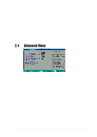
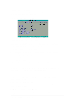
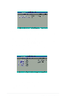
The SDRAM parameters (items 2~5) become configurable only when you set the SDRAM Configuration to [User Defined]. SDRAM CAS Latency [3T] This item controls the latency between the SDRAM read command and the time the data actually becomes available. SDRAM RAS to CAS Delay [4T] This item controls the latency between the DDR SDRAM active command and the read/write command. SDRAM RAS Precharge Time [4T] This item controls the idle clocks after issuing a precharge command to the DDR SDRAM. SDRAM RAS Active Time [7T] This item controls the number of DDR SDRAM clocks used for DDR SDRAM parameters. Graphics Aperture Size [64MB] This feature allows you to select the size of mapped memory for AGP graphic data. Configuration options: [4MB] [8MB] [16MB] [32MB] [64MB] [128MB] [256MB] [512MB] Onboard VGA Shared Memory Size [32MB] This field allows you set the onboard VGA shared memory size with the currently installed memory. Configuration options: [8MB] [16MB] [32MB] [64MB] Video Memory Cache Mode [UC] USWC (uncacheable, speculative write combining) is a new cache technology for the video memory of the processor. It can greatly improve the display speed by caching the display data. You must set this to UC (uncacheable) if your display card does not support this feature, otherwise the system may not boot. Configuration options: [UC] [USWC] Delayed Transaction [Enabled] When set to [Enabled], this feature frees the PCI bus when the CPU is accessing 8-bit ISA cards. This process normally consumes about 50-60 PCI clocks without PCI delayed transaction. Set this field to [Disabled] when using ISA cards that are not PCI 2.1 compliant. Configuration options: [Enabled] [Disabled] Onboard PCI IDE Enable [Both] This field allows you to enable either the primary IDE channel or secondary IDE channel, or both. You can also set both channels to [Disabled]. Configuration options: [Both] [Primary] [Secondary] [Disabled] ASUS A7S266-VM/U2 Motherboard 2-17
-
 1
1 -
2
-
3
-
4
-
5
-
6
-
7
-
8
-
9
-
10
-
11
-
12
-
13
-
14
-
15
-
16
-
17
-
18
-
19
-
20
-
21
-
22
-
23
-
24
-
25
-
26
-
27
-
28
-
29
-
30
-
31
-
32
-
33
-
34
-
35
-
36
-
37
-
38
-
39
-
40
-
41
-
 42
42 -
 43
43 -
 44
44 -
 45
45 -
 46
46 -
 47
47 -
 48
48 -
 49
49 -
 50
50 -
 51
51 -
 52
52 -
53
-
54
-
55
-
56
-
57
-
58
-
59
-
60
 |
 |