Asus a7n8xx Motherboard DIY Troubleshooting Guide - Page 16
Motherboard layout - a7n8x x bios
 |
View all Asus a7n8xx manuals
Add to My Manuals
Save this manual to your list of manuals |
Page 16 highlights
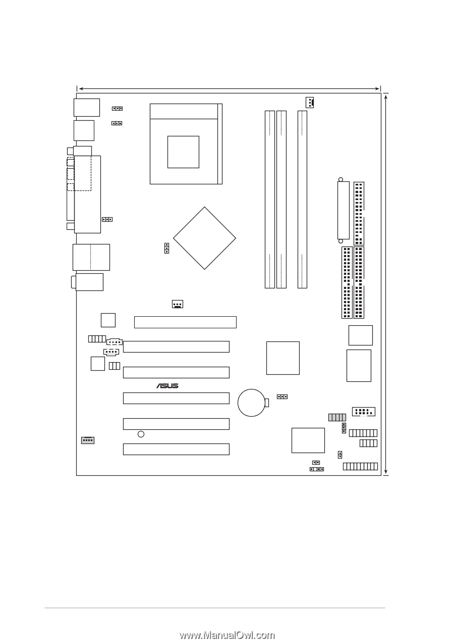
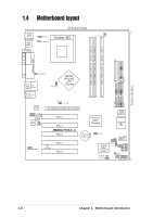
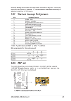
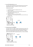
30.5cm (12.0in) 1.4 Motherboard layout PS/2 T: Mouse B: Keyboard USB3 USB4 COM1 24.5cm (9.64in) KBPWR1 USBPWR_34 Socket 462 CPU_FAN1 ATX Power Connector DDR DIMM1 (64/72 bit, 184-pin module) DDR DIMM2 (64/72 bit, 184-pin module) DDR DIMM3 (64/72 bit, 184-pin module) PARALLEL PORT FLOPPY1 USBPWR_12 Bottom: USB1 USB2 Top: RJ-45 Top:Line In Center:Line Out Below:Mic In CPU_FSB nVidia nForce2 400 Chipset 0 1 23 4 5 PRI_IDE1 SEC_IDE1 CHA_FAN1 Realtek RTL8201 CD1 FPAUDIO1 AUX1 Audio Codec SPDIF1 Accelerated Graphics Port (AGP) PCI 1 PCI 2 ®A7N8X-X PCI 3 nForce2 MCP Chipset CR2032 3V Lithium Cell CMOS Power CLRTC1 2Mb BIOS Super I/O USB56 COM2 MODEM1 PWR_LED1 PCI 4 PCI 5 USBPWR_56 ASUS ASIC with Hardware Monitor GAME1 IR_CON1 IDELED1 PWRTMP1 CHASSIS1 CTRL_PANEL1 1-6 Chapter 1: Motherboard Information
-
 1
1 -
2
-
3
-
4
-
5
-
6
-
7
-
8
-
9
-
10
-
 11
11 -
 12
12 -
 13
13 -
 14
14 -
 15
15 -
 16
16 -
 17
17 -
 18
18 -
 19
19 -
 20
20 -
 21
21 -
22
-
23
-
24
-
25
-
26
-
27
-
28
-
29
-
30
-
31
-
32
-
33
-
34
-
35
-
36
-
37
-
38
-
39
-
40
-
41
-
42
-
43
-
44
-
45
-
46
-
47
-
48
-
49
-
50
-
51
-
52
-
53
-
54
-
55
-
56
-
57
-
58
-
59
-
60
 |
 |