Foxconn A9DA English Manual. - Page 39
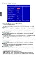
► Memory Configuration / DRAM Timing Configuration
 |
View all Foxconn A9DA manuals
Add to My Manuals
Save this manual to your list of manuals |
Page 39 highlights
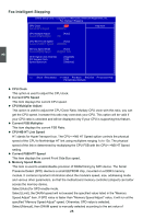
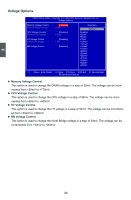
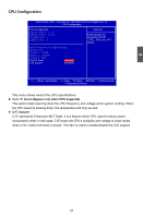
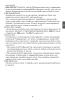
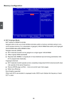
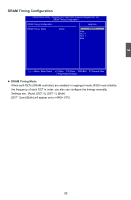
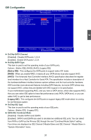
Advanced Chipset Features CMOS Setup Utility - Copyright (C) 1985-2006, American Megatrends, Inc. Advanced Chipset Features Northbridge Chipset Configuration Help Item ► Memory Configuration [Press Enter] ► DRAM Timing Configuration [Press Enter] CAS Latency :9 CLK, N/A RAS/CAS Delay :9 CLK, N/A Row Precharge Time :9 CLK, N/A Min Active RAS :24 CLK, N/A RAS/RAS Delay :4 CLK, N/A Row Cycle :33 CLK, N/A Internal Graphics Configuration Internal Graphics Mode UMA Frame Buffer Size Primary Video Controller Surround View AMD 880 HD Audio [UMA] [Auto] [PCI-GFX0-IGFX] [Auto] [Enabled] Move Enter:Select +/-/:Value F10:Save ESC:Exit F1:General Help F9:Optimized Defaults ► Memory Configuration / DRAM Timing Configuration Press to go to its submenu. 3 The following six items display the values configured at the settings of "DRAM Timing Mode". ► CAS Latency This item shows the CAS latency. The CAS Latency is the number of clock cycles that elapse from the time the request for data is sent to the actual memory location until the data is transmitted from the module. ► RAS / CAS Delay This item displays a delay time (in clock cycles) between the CAS and RAS strobe signals. ► Row Precharge Time This item shows the number of clock cycles taken between issuing of the precharge command and the active command. The DRAM row precharge time is in unit of clock cycle. ► Min Active RAS Displays the number of clock cycles taken between a bank active command and issuing of the precharge command. ► RAS / RAS Delay This item displays a delay time (in clock cycles) between the RAS and RAS strobe signals. ► Row Cycle This item shows the minimum timing interval between successive active commands to the same bank. The row cycle time is in unit of clock cycle. ► Internal Graphics Mode It allows you to determine whether to allocate memory for the integrated graphics controller from the system memory or SidePort memory. Options: [Disabled], [UMA], [UMA+SIDEPORT]. [Disabled]- Disables the integrated graphics controller. [UMA]-In UMA mode, the only memory to which the integrated graphics has access is a dynamically allocated partition of system memory. The size of the parition is selectable from 32
-
 1
1 -
2
-
3
-
4
-
5
-
6
-
7
-
8
-
9
-
10
-
11
-
12
-
13
-
14
-
15
-
16
-
17
-
18
-
19
-
20
-
21
-
22
-
23
-
24
-
25
-
26
-
27
-
28
-
29
-
30
-
31
-
32
-
33
-
 34
34 -
 35
35 -
 36
36 -
 37
37 -
 38
38 -
 39
39 -
 40
40 -
 41
41 -
 42
42 -
 43
43 -
 44
44 -
45
-
46
-
47
-
48
-
49
-
50
-
51
-
52
-
53
-
54
-
55
-
56
-
57
-
58
-
59
-
60
-
61
-
62
-
63
-
64
-
65
-
66
-
67
-
68
-
69
-
70
-
71
-
72
-
73
-
74
-
75
-
76
-
77
-
78
-
79
-
80
-
81
-
82
-
83
-
84
-
85
-
86
-
87
-
88
-
89
-
90
-
91
-
92
-
93
-
94
-
95
-
96
-
97
-
98
-
99
-
100
-
101
-
102
-
103
-
104
-
105
-
106
-
107
-
108
-
109
-
110
-
111
-
112
-
113
-
114
-
115
 |
 |