Gigabyte GA-G1975X Manual - Page 8
Block Diagram - overclock
 |
View all Gigabyte GA-G1975X manuals
Add to My Manuals
Save this manual to your list of manuals |
Page 8 highlights
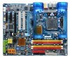
Block Diagram 2 PCI-ECLK (100MHz) LGA775 Processor CPUCLK+/-(266/200 MHz) PCI Express x16 Host Interface DDRII 888(Note 1)/ 667 (Note 2)/ 533MHz DIMM Intel® 975X Dual Channel Memory MCHCLK (266/200MHz) 2 PCI Express x 4 LAN1 RJ45 PCI-ECLK (100MHz) x4/x1 Broadcom 5789 x4/x1 x1 PCI Express Bus PCI Bus TSB43AB23 IT8211F Intel® ICH7R CREATIVE CA0106 2 PCI 8 USB Ports Dual BIOS 4 SATA 3Gb/s ATA33/66/100 IDE Channel IT8712 Floppy COM Port PS/2 KB/Mouse 24MHz 33MHz PCICLK(33MHz) 3 IEEE1394a ATA33 / 66 / 100 / 133 IDE Channel Surround Speaker Out Center/Subwoofer Speaker Out Side Speaker Out MIC Line-Out Line-In SPDIF In SPDIF Out (Note 1) DDR II memory can be overclocked to 888MHz (must be used with a 1066MHz FSB processor) through overclocking in BIOS. Go to GIGABYTE's website for more information about the supported DDR II memory modules for this feature. (Note 2) To use a DDR II 667 memory module on the motherboard, you must install an 800/1066MHz FSB processor. - 8 -
-
 1
1 -
2
-
 3
3 -
 4
4 -
 5
5 -
 6
6 -
 7
7 -
 8
8 -
 9
9 -
 10
10 -
 11
11 -
 12
12 -
 13
13 -
14
-
15
-
16
-
17
-
18
-
19
-
20
-
21
-
22
-
23
-
24
-
25
-
26
-
27
-
28
-
29
-
30
-
31
-
32
-
33
-
34
-
35
-
36
-
37
-
38
-
39
-
40
-
41
-
42
-
43
-
44
-
45
-
46
-
47
-
48
-
49
-
50
-
51
-
52
-
53
-
54
-
55
-
56
-
57
-
58
-
59
-
60
-
61
-
62
-
63
-
64
-
65
-
66
-
67
-
68
-
69
-
70
-
71
-
72
-
73
-
74
-
75
-
76
-
77
-
78
-
79
-
80
-
81
-
82
-
83
-
84
-
85
-
86
-
87
-
88
-
89
-
90
-
91
-
92
-
93
-
94
-
95
-
96
-
97
-
98
-
99
-
100
-
101
-
102
-
103
-
104
-
105
-
106
-
107
-
108
-
109
-
110
-
111
-
112
 |
 |
