Gigabyte GA-G1975X Manual - Page 1
Gigabyte GA-G1975X Manual
 |
View all Gigabyte GA-G1975X manuals
Add to My Manuals
Save this manual to your list of manuals |
Page 1 highlights
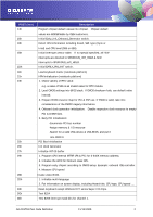
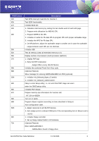
GA-G1975X Post Code Definition AWARD Post Code Definition POST (hex) CFh C0h Description Test CMOS R/W functionality. Early chipset initialization: -Disable shadow RAM -Disable L2 cache (socket 7 or below) -Program basic chipset registers C1h 1. Detect memory -Auto-detection of DRAM size, type and ECC. -Auto-detection of L2 cache (socket 7 or below) 2. PEG slots Auto-Configuration C3h Expand compressed BIOS code to DRAM C5h Call chipset hook to copy BIOS back to E000 & F000 shadow RAM. 0h1 Expand the Xgroup codes locating in physical address 1000:0 03h Initial Superio_Early_Init switch. 05h 1. Blank out screen 2. Clear CMOS error flag 07h 1. Clear 8042 interface 2. Initialize 8042 self-test 08h 1. Test special keyboard controller for Winbond 977 series Super I/O chips. 2. Enable keyboard interface. 0Ah 1. Disable PS/2 mouse interface (optional). 2. Auto detect ports for keyboard & mouse followed by a port & interface swap (optional). 3. Reset keyboard for Winbond 977 series Super I/O chips. 0Eh Test F000h segment shadow to see whether it is R/W-able or not. If test fails, keep beeping the speaker. 10h Auto detect flash type to load appropriate flash R/W codes into the run time area in F000 for ESCD & DMI support. 12h Use walking 1's algorithm to check out interface in CMOS circuitry. Also set real-time clock power status, and then check for override. GA-G1975X Post Code Definition 11/14/2005 1
-
 1
1 -
 2
2 -
 3
3 -
 4
4 -
 5
5
 |
 |