Intel AXXROMBSASMR Hardware User Guide - Page 23
Intel® Integrated RAID Module SROMBSASMR Characteristics
 |
View all Intel AXXROMBSASMR manuals
Add to My Manuals
Save this manual to your list of manuals |
Page 23 highlights
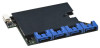
3 Intel® Integrated RAID Module SROMBSASMR Characteristics LSI J7 J6 J1- J4 J8 J5 AF003065 Figure 4. Card Layout Table 1. Jumper Description s Jumper Description Type Comments J1 - J4 J5 J6 J7 J8 Internal SAS/SATA Port Connectors, Ports 0-3 Board-to-board connector for 20-pin connector Battery Backup Unit Universal Asynchronous Receiver/Transmitter (UART) Keyed I2C Connector 4-pin connector 3-pin keyed connector Debug Connector 4-pin connector Connection to SAS/SATA devices: • J1 = SAS/SATA Port 0 • J2 = SAS/SATA Port 1 • J3 = SAS/SATA Port 2 • J4 = SAS/SATA Port 3 Provides an interface to the daughter card that contains the battery backup unit. Not populated and should not be used. Out-of-band enclosure management (SES2) Reserved Intel® Integrated RAID Module SROMBSASMR Hardware User's Guide 13
-
 1
1 -
2
-
3
-
4
-
5
-
6
-
7
-
8
-
9
-
10
-
11
-
12
-
13
-
14
-
15
-
16
-
17
-
 18
18 -
 19
19 -
 20
20 -
 21
21 -
 22
22 -
 23
23 -
 24
24 -
 25
25 -
 26
26 -
 27
27 -
 28
28 -
29
-
30
-
31
-
32
-
33
-
34
-
35
-
36
-
37
-
38
-
39
-
40
 |
 |
