Intel DC3217BY Technical Product Specification - Page 9
Intel DC3217BY Manual
 |
View all Intel DC3217BY manuals
Add to My Manuals
Save this manual to your list of manuals |
Page 9 highlights
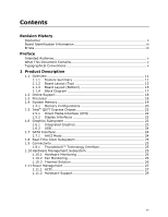
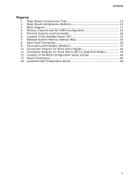
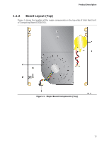
Contents Figures 1. Major Board Components (Top 13 2. Major Board Components (Bottom 15 3. Block Diagram 17 4. Memory Channel and SO-DIMM Configuration 21 5. Thermal Solution and Fan Header 26 6. Location of the Standby Power LED 31 7. Detailed System Memory Address Map 34 8. Back Panel Connectors 36 9. Connectors and Headers (Bottom 37 10. Connection Diagram for Front Panel Header 42 11. Connection Diagram for Front Panel USB 2.0 Dual-Port Header 43 12. Location of the BIOS Configuration Setup Jumper 44 13. Board Dimensions 46 14. Localized High Temperature Zones 49 ix
-
 1
1 -
2
-
3
-
 4
4 -
 5
5 -
 6
6 -
 7
7 -
 8
8 -
 9
9 -
 10
10 -
 11
11 -
 12
12 -
 13
13 -
 14
14 -
15
-
16
-
17
-
18
-
19
-
20
-
21
-
22
-
23
-
24
-
25
-
26
-
27
-
28
-
29
-
30
-
31
-
32
-
33
-
34
-
35
-
36
-
37
-
38
-
39
-
40
-
41
-
42
-
43
-
44
-
45
-
46
-
47
-
48
-
49
-
50
-
51
-
52
-
53
-
54
-
55
-
56
-
57
-
58
-
59
-
60
-
61
-
62
-
63
-
64
-
65
-
66
-
67
-
68
-
69
-
70
-
71
-
72
-
73
-
74
-
75
-
76
-
77
-
78
-
79
-
80
-
81
-
82
 |
 |

Contents
ix
Figures
1.
Major Board Components (Top)
..........................................................
13
2.
Major Board Components (Bottom)
.....................................................
15
3.
Block Diagram
..................................................................................
17
4.
Memory Channel and SO-DIMM Configuration
......................................
21
5.
Thermal Solution and Fan Header
.......................................................
26
6.
Location of the Standby Power LED
.....................................................
31
7.
Detailed System Memory Address Map
................................................
34
8.
Back Panel Connectors
......................................................................
36
9.
Connectors and Headers (Bottom)
......................................................
37
10. Connection Diagram for Front Panel Header
.........................................
42
11. Connection Diagram for Front Panel USB 2.0 Dual-Port Header
...............
43
12. Location of the BIOS Configuration Setup Jumper
.................................
44
13. Board Dimensions
.............................................................................
46
14. Localized High Temperature Zones
.....................................................
49