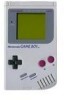
Nintendo DMG-01 Manual
Nintendo DMG-01 - Game Boy Console Manual
 |
View all Nintendo DMG-01 manuals
Add to My Manuals
Save this manual to your list of manuals |
Nintendo DMG-01 manual content summary:
- Nintendo DMG-01 | Manual - Page 1
Game BoyTM CPU Manual Sources by: Pan of Anthrox, GABY, Marat Fayzullin, Pascal Felber, A5 SIZE PAPER (148mm x 210mm)! Note: Game BoyTM, Game Boy PocketTM, Super Game BoyTM and Game Boy ColorTM are registered trademarks of Nintendo CO., LTD. © 1989 to 1999 by Nintendo CO., LTD. Version: 1.01 by DP - Nintendo DMG-01 | Manual - Page 2
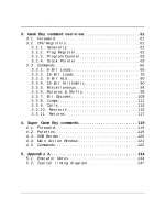
1. Foreword Game BoyTM CPU Manual Table of Contents 1. Foreword 4 2. Hardware specifications 5 2.1. Forward 5 2.2. Terms 5 2.3. Game Boy Specs 6 2.8.3. Sprite RAM Bug 27 2.9. Sound 28 2.10. Timer 30 2.11. Serial I/O 31 2.12. Interrupts 32 2.12.1. Interrupt Procedure 32 2.12.2. Interrupt - Nintendo DMG-01 | Manual - Page 3
BoyTM CPU Manual 1. Foreword 3. Game Boy command overview 61 3.1. Foreword 61 3.2. CPU Registers 61 3.2.1. Generally 61 111 3.3.9. Calls 114 3.3.10. Restarts 116 3.3.11. Returns 117 4. Super Game Boy commands 119 4.1. Foreword 119 4.2. Palettes 119 4.3. SGB Border 120 4.4. Main - Nintendo DMG-01 | Manual - Page 4
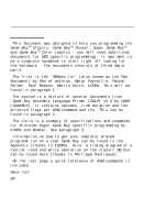
Language Primer (GALP) V1.0'by GABY (GAmeBoY). It contains opcodes, time duration and the affected flags per ASM command and the. This can be found in paragraph 2. The third is a summary of specifications and commands for Nintendo Super Game Boy speciffic programming by kOOPa and Bowser. See - Nintendo DMG-01 | Manual - Page 5
the inner workings on the hand-held game machine known as Game Boy, manufactured and designed by Nintendo Co., LTD. This info is presented to inform a user on how their Game Boy works and what makes it "tick". GameBoy is copyrighted by Nintendo Co., LTD. Any reference to copyrighted material - Nintendo DMG-01 | Manual - Page 6
2.3. Game Boy Specs Game BoyTM CPU Manual 2.3. Game Boy Specs • CPU: 8-bit (Similar to the Z80 processor.) • Main RAM: 8K Byte • Video RAM: 8K Byte • Screen Size 2.6" • Resolution: 160x144 (20x18 tiles) • Max # of sprites: - Nintendo DMG-01 | Manual - Page 7
Game BoyTM CPU Manual 2.4. Processor have been added and some have been taken away. The following are added instructions: ADD SP,nn LDI (HL),A LDD (HL),A LDI A,(HL) LDD A,(HL) LD A,($FF00+nn) LD A,($FF00+C) LD ($FF00+nn),A LD ($FF00+C),A LD (nnnn),SP LD - Nintendo DMG-01 | Manual - Page 8
2.5. Memory Map Game BoyTM CPU Manual 2.5. Memory Map 2.5.1. General memory map Interrupt Enable Register FFFF Internal RAM FF80 Empty but unusable for I/O 16kB switchable ROM bank | 4000 |= 32kB Cartrigbe 16kB ROM bank #0 | 0000 -- * NOTE: b = bit, B = byte Page 8 V 1.01 - Nintendo DMG-01 | Manual - Page 9
Game BoyTM CPU Manual 2.5.2. Echo of 8kB Internal RAM 2.5.2. Echo of 8kB Internal RAM The addresses E000-FE00 To use them you must first put the MBC1 into 4MbitROM/32KbyteRAM mode by writing 01 to 6000. The two least significant bits you write to 4000 will then be output to these pins. by DP Page - Nintendo DMG-01 | Manual - Page 10
2.5.4. Reserved Memory Locations Game BoyTM CPU Manual 2.5.4. Reserved Memory Locations 0000 0008 Address 0050 Timer Overflow Interrupt Start Address 0058 0060 Serial Transfer Completion Interrupt Start Address High-to-Low of P10 is a NOP and a JP instruction here but not always. Page 10 - Nintendo DMG-01 | Manual - Page 11
Game BoyTM CPU Manual Locations 2.5.4. Reserved Memory 0104-0133 Scrolling Nintendo graphic: CE ED 66 normally $00 if [$014B] $33.) 0146 GB/SGB Indicator (00 = GameBoy, 03 = Super GameBoy functions) (Super GameBoy functions won't work if $03.) 0147 Cartridge type: 0-ROM ONLY 12-ROM - Nintendo DMG-01 | Manual - Page 12
2.5.4. Reserved Memory Locations Game BoyTM CPU Manual F-ROM+MBC3+TIMER+BATT FF - Hudson HuC-1 10-ROM+MBC3+TIMER+RAM+BATT 11-ROM+MBC3 Check 0144/0145 for Licensee code. 79 - Accolade A4 - Konami (Super GameBoy function won't work if $33.) 014C Mask ROM Version number (Usually $00) Page 12 - Nintendo DMG-01 | Manual - Page 13
Game BoyTM CPU Manual checksum bytes and taking two lower bytes of the result. (GameBoy ignores this value.) 2.6. Cartridge Types The following define the value (XXXXXXXS - X = Don't care, S = Memory model select) into 6000-7FFF area will select the memory model to use. S = 0 selects 16/8 mode. S = - Nintendo DMG-01 | Manual - Page 14
2.6. Cartridge Types Game BoyTM CPU Manual Rom bank 0 is not accessible from 4000-7FFF and can only be read from 0000-3FFF. If memory model is set to during power down of the GameBoy. (NOTE: Nintendo suggests values $0A to enable and $00 to disable RAM bank!!) If memory model is set to 16/8 mode 01 - Nintendo DMG-01 | Manual - Page 15
Game BoyTM CPU Manual Clock (RTC) not found in any other MBC. Some MBC3 carts do not support it (WarioLand II non color version) but some do (Harvest Moon/Japanese version controller is the first MBC that is guaranteed to run in GameBoy Color double-speed mode but it appears the other MBC's run fine - Nintendo DMG-01 | Manual - Page 16
2.6. Cartridge Types Game BoyTM CPU Manual It is similar to the MBC3 (but no RTC) but can made by Hudson Soft appears to be very similar to an MBC1 with the main difference being that it supports infrared LED input / output. The Japanese cart "Fighting Phoenix" (internal cart name: SUPER B DAMAN) - Nintendo DMG-01 | Manual - Page 17
Game BoyTM CPU Manual 2.7. Special modi 2.7. Special modi 2.7.1. Power Up Sequence When the GameBoy is powered up, a 256 byte program starting at memory location 0 is executed. This program is located in a ROM inside the GameBoy. The first thing the program does is read the cartridge locations - Nintendo DMG-01 | Manual - Page 18
2.7.1. Power Up Sequence Game BoyTM CPU Manual BC=$0013 DE=$00D8 HL=$014D Stack Pointer=$FFFE [$FF05] = $00 ; TIMA [$FF06] = $00 ; TMA [$FF07] = $00 ; TAC [$FF10] = $80 ] = $FC ; BGP [$FF48] = $FF ; OBP0 [$FF49] = $FF ; OBP1 [$FF4A] = $00 ; WY [$FF4B] = $00 ; WX [$FFFF] = $00 ; IE Page 18 V 1.01 - Nintendo DMG-01 | Manual - Page 19
Game BoyTM CPU Manual 2.7.1. Power Up Sequence It is not a good idea to assume the above values will always exist. A later version GameBoy could contain different values than these at reset. Always set these registers on reset rather than assume they are as above. Please note that GameBoy internal - Nintendo DMG-01 | Manual - Page 20
. This instruction skipping doesn't occur when interrupts are enabled (EI). This "skipping" does not seem to occur on the GameBoy Color even in regular GB mode. ($143=$00) EXAMPLES from Martin Korth who documented this problem: (assuming interrupts disabled for all examples) 1) This code - Nintendo DMG-01 | Manual - Page 21
Game BoyTM CPU Manual 2.7.3. Low-Power Mode FA FA 34 12 ld a,(34FA) ld (de),a to be repeated once, the second HALT wouldn't lock the cpu. Below is suggested code for Game Boy programs: ; **** Main Game Loop **** Main: halt ; stop system clock ; return from halt when ; interrupted nop ; - Nintendo DMG-01 | Manual - Page 22
Game BoyTM CPU Manual ; **** V-Blank Interrupt Routine **** Vblnk: push af push bc push de push hl call SpriteDma ; Do sprite updates ld a,1 ld (VblnkFlag),a pop hl pop de pop bc pop af reti 2.8. Video 2.8.1. Tiles The main GameBoy around the screen (i.e. when part of it goes off the - Nintendo DMG-01 | Manual - Page 23
Game BoyTM CPU Manual 2.8.1. Tiles number of a tile to be displayed. Tile patterns are taken from the Tile Data Table located either at $8000-8FFF or $8800-97FF. In - Nintendo DMG-01 | Manual - Page 24
2.8.1. Tiles Game BoyTM CPU Manual WX may be changed during a scan line interrupt (to either cause a graphic distortion effect or to disable the window (WX>166) ) but second table can be used for the background and the window display and its tiles are numbered from -128 to 127. Page 24 V 1.01 - Nintendo DMG-01 | Manual - Page 25
Game BoyTM CPU Manual 2.8.2. Sprites 2.8.2. Sprites GameBoy video controller can display up to 40 sprites either in 8x8 or in 8x16 pixels. Because of a limitation of hardware, only ten sprites can be - Nintendo DMG-01 | Manual - Page 26
2.8.2. Sprites Game BoyTM CPU Manual To display a sprite in the upper left corner of the screen set sprite X=8, Y=16. Only 10 sprites can be displayed on any one is flipped vertically if this bit is set to 1. X flip Sprite pattern is flipped horizontally if this bit is set to 1. Page 26 V 1.01 - Nintendo DMG-01 | Manual - Page 27
Game BoyTM CPU Manual 2.8.2. Sprites Bit4 Palette number Sprite colors are taken from OBJ1PAL if this bit is set to 1 and from OBJ0PAL otherwise. 2.8.3. Sprite RAM Bug There is a flaw in the GameBoy (hl),a Only sprites 1 & 2 ($FE00 & $FE04) are not affected by these instructions. by DP Page 27 - Nintendo DMG-01 | Manual - Page 28
Game BoyTM CPU Manual 2.9. Sound There are two sound channels connected to the output terminals SO1 and SO2. There is also a input terminal Vin connected to the cartridge. It can be routed to either of both output terminals. GameBoy By initializing sound 3, it starts it's function. Page 28 V 1.01 - Nintendo DMG-01 | Manual - Page 29
Game BoyTM CPU Manual 2.9. Sound When the All Sound OFF flag (bit 7 of NR52) is set to 0, the mode registers for sounds 1,2,3, and 4 are reset and the sound output - Nintendo DMG-01 | Manual - Page 30
10. Timer Game BoyTM CPU Manual 2.10. Timer Sometimes it's useful to have a timer that interrupts at regular intervals for routines that require periodic or percise updates. The timer in the GameBoy has a selectable FF07),a ;Set TMA to divide clock by 4 ;Set clock to 262144 Hertz Page 30 V 1.01 - Nintendo DMG-01 | Manual - Page 31
Game BoyTM CPU Manual 2.11. Serial I/O 2.11. Serial I/O The serial I/O port on the Gameboy is a very simple setup and is crude compared to standard RS-232 (IBMPC) or RS-485 (Macintosh) serial ports. There are no start or stop bits so the programmer must be more creative when using this port. - Nintendo DMG-01 | Manual - Page 32
Serial I/O Game BoyTM CPU Manual allows a certain amount of synchronization with each serial port. The state of the last bit shifted out determines the state of the output line until another transfer takes place. If a serial transfer with internal clock is performed and no external GameBoy V 1.01 - Nintendo DMG-01 | Manual - Page 33
Game BoyTM CPU Manual 2.12.1. Interrupt Procedure Resetting of the IF register, which was the cause of the interrupt, is done by hardware. During the interrupt, pushing of registers to be used should be performed by the interrupt routine. Once the interrupt service is in progress, all the - Nintendo DMG-01 | Manual - Page 34
2.12.2. Interrupt Descriptions Game BoyTM CPU Manual 2.12.2. Interrupt Descriptions The following interrupts only occur if they have been enabled in the Interrupt Enable register ($FFFF) and if the interrupts have actually been enabled using the EI instruction. 1. V-Blank The V-Blank interrupt - Nintendo DMG-01 | Manual - Page 35
Game BoyTM CPU Manual 2.12.2. Interrupt Descriptions 5. High-to-Low of P10-P13 This interrupt occurs on a transition of any of the keypad input lines from high to low. - Nintendo DMG-01 | Manual - Page 36
Game BoyTM CPU Manual This is the matrix layout for register $FF00: P14 P15 | | P10-------O-Right----O-A | | P11-------O-Left-----O-B | | P12-------O-Up-------O-Select | | P13-------O-Down-----O-Start | | Example code: Game setting it low - Nintendo DMG-01 | Manual - Page 37
Game BoyTM CPU Manual 2.13.1. I/O Registers CPL AND $0F OR B LD B,A LD A,($FF8B) XOR B AND and Up. The value returned in accumulator A would be $94. 2. FF01 (SB) Name - SB Contents - Serial transfer data (R/W) 8 Bits of data to be read/written 3. FF02 (SC) Name - SC Contents - SIO control - Nintendo DMG-01 | Manual - Page 38
2.13.1. I/O Registers Game BoyTM CPU Manual Bit 7 - Transfer Start Flag 0: Non transfer 1: Start and is automatically set to 0 at the end of Transfer. Transmitting and receiving serial data is done simultaneously. The received data is automatically stored in SB. 4. it overflows. Page 38 V 1.01 - Nintendo DMG-01 | Manual - Page 39
Game BoyTM CPU Manual 2.13 1: Start Timer Bits 1+0 - Input Clock Select 00: 4.096 KHz (~4.194 KHz SGB) 01: 262.144 Khz (~268.4 KHz SGB) 10: 65.536 KHz (~67.11 KHz SGB 4: Transition from High to Low of Pin number P10-P13 Bit 3: Serial I/O transfer complete Bit 2: Timer Overflow Bit 1: LCDC (see STAT - Nintendo DMG-01 | Manual - Page 40
2.13.1. I/O Registers Game BoyTM CPU Manual interrupts are: Interrupt V-Blank LCDC Status Priority 1 2 Timer Overflow 3 Serial Transfer 4 Hi-Lo of P10-P13 5 Start Address $0040 $0048 - Modes 0, 1, 2 change 001: 7.8 ms (1/128Hz) 010: 15.6 ms (2/128Hz) 011: 23.4 ms (3/128Hz) Page 40 V 1.01 - Nintendo DMG-01 | Manual - Page 41
Game BoyTM CPU Manual 2.13.1. I/O Registers 100: 31.3 ms (4/128Hz) 101: 39.1 ms (5/128Hz) 110: 46.9 ms (6/128Hz) 111: 7-6 - Wave Pattern Duty Bit 5-0 - Sound length data (t1: 0-63) Wave Duty: (default: 10) 00: 12.5 01: 25 10: 50 11: 75 Sound Length = (64-t1)*(1/256) seconds by DP Page 41 - Nintendo DMG-01 | Manual - Page 42
2.13.1. I/O Registers Game BoyTM CPU Manual 11. FF12 (NR12) Name - NR 12 Contents - Sound Mode 1 register, Envelope (R/W) Bit 7-4 - Initial volume of envelope Bit 3 - Only Bit 6 can be read. Bit 7 - Initial (when set, sound restarts) Bit 6 - Counter/consecutive selection Page 42 V 1.01 - Nintendo DMG-01 | Manual - Page 43
Game BoyTM CPU Manual 2.13.1. I/O Registers Bit 2-0 - Frequency's higher 3 bits (x) Frequency = 4194304/(32*(2048-x)) Hz = 131072 pattern duty Bit 5-0 - Sound length data (t1: 0-63) Wave Duty: (default: 10) 00: 12.5 01: 25 10: 50 11: 75 Sound Length = (64-t1)*(1/256) seconds by DP Page 43 - Nintendo DMG-01 | Manual - Page 44
2.13.1. I/O Registers Game BoyTM CPU Manual 15. FF17 (NR 22) Name - NR 22 Contents - Sound Mode 2 register, envelope (R/W) Bit 7-4 - Initial volume of envelope Bit 3 - Sound Mode 2 register, frequency hi data (R/W) Only bit 6 can be read. Bit 7 - Initial (when set, sound Page 44 V 1.01 - Nintendo DMG-01 | Manual - Page 45
Game BoyTM CPU Manual 2.13.1. I/O Registers restarts) Bit 6 - Counter/consecutive selection Bit 2-0 - Frequency's higher 3 bits (x) Frequency = 4194304/(32*(2048-x)) Hz = 131072/(2048-x) Hz Counter/consecutive Selection 0 = Regardless of the - Nintendo DMG-01 | Manual - Page 46
I/O Registers Game BoyTM CPU Manual 20. FF1C (NR 32) Name - NR 32 Contents - Sound Mode 3 register, Select output level (R/W) Only bits 6-5 can be read Bit 6-5 - Select output level 00: Mute 01: Produce Wave 3 register, frequency's higher data (R/W) Only bit 6 can be read. Page 46 V 1.01 - Nintendo DMG-01 | Manual - Page 47
Game BoyTM CPU Manual 2.13.1. I/O Registers Bit 7 - Initial (when set,sound restarts) Bit 6 - Counter/consecutive flag Bit 2-0 - Frequency's higher 3 bits (x). Frequency = 4194304/(64*(2048-x)) Hz = 65536/(2048-x) Hz Counter/ - Nintendo DMG-01 | Manual - Page 48
2.13.1. I/O Registers Game BoyTM CPU Manual Bit 2-0 - Number of envelope sweep (n: 0-7) (If zero, : f * 1/2^3 * 1/3 100: f * 1/2^3 * 1/4 101: f * 1/2^3 * 1/5 110: f * 1/2^3 * 1/6 111: f * 1/2^3 * 1/7 f = 4.194304 Mhz Selection of the polynomial counter step: 0: 15 steps 1: 7 steps Page 48 V 1.01 - Nintendo DMG-01 | Manual - Page 49
Game BoyTM CPU Manual 2.13.1. I/O Registers Selection of the shift clock frequency of the polynomial counter: 0000: dividing ratio of frequencies * 1/2 0001: dividing ratio of frequencies * 1/2^2 0010: dividing ratio - Nintendo DMG-01 | Manual - Page 50
2.13.1. I/O Registers Game BoyTM CPU Manual 27. FF24 (NR 50) Name - NR 50 Contents - Channel control / ON-OFF / Volume (R/W) Bit 7 - Vin->SO2 ON/OFF Bit 6-4 - SO2 - Output sound 3 to SO1 terminal Bit 1 - Output sound 2 to SO1 terminal Bit 0 - Output sound 1 to SO1 terminal Page 50 V 1.01 - Nintendo DMG-01 | Manual - Page 51
Game BoyTM CPU Manual 2.13.1. I/O Registers 29. FF26 (NR 52) Name - NR 52 (Value at reset: $F1-GB, $F0-SGB) Contents - Sound on/off (R/W) Bit 7 - All sound on/off 0: - Nintendo DMG-01 | Manual - Page 52
2.13.1. I/O Registers Game BoyTM CPU Manual 0: Stop completely (no picture on screen) 1: operation Bit 6 - Window Tile Map Display Select 0: $9800-$9BFF 1: $9C00-$9FFF Bit 5 - Window (STAT) Name - STAT Contents - LCDC Status (R/W) Bits 6-3 - Interrupt Selection By LCDC Status Page 52 V 1.01 - Nintendo DMG-01 | Manual - Page 53
Game BoyTM CPU Manual 2.13.1. I/O Registers Bit 6 - LYC=LY Coincidence (Selectable) Bit 5 - Mode 10 Bit 4 - Mode 01 Bit 3 - Mode 00 0: Non Selection 1: Selection Bit 2 - Coincidence Flag 0: LYC not equal to LCDC LY 1: LYC = LCDC LY Bit 1-0 - Mode Flag 00: During H-Blank 01: During V-Blank 10: - Nintendo DMG-01 | Manual - Page 54
2.13.1. I/O Registers Game BoyTM CPU Manual Mode 0: 000___000___000___000___000___000___000 Mode 1 11111111111111__ Mode 2: ___2_____2_____2_____2_____2_____2 2_ Mode 3: ____33____33____33____33____33____33 3 The Y (R/W) 8 Bit value $00-$FF to scroll BG Y screen position. Page 54 V 1.01 - Nintendo DMG-01 | Manual - Page 55
CPU Manual 2.13.1. I/O Registers 34. FF43 (SCX) Name - SCX Contents - Scroll X (R/W) 8 Bit value $00-$FF to scroll BG X screen position. 35. FF44 (LY) Name - LY Contents - LCDC Y-Coordinate (R) The LY indicates the vertical line to which the present data is transferred to the LCD Driver - Nintendo DMG-01 | Manual - Page 56
2.13.1. I/O Registers Game BoyTM CPU Manual can be performed. It takes 160 microseconds for the transfer. 40*28 bit = #140 or #$8C. As you can see, it only must be copied & executed in high ram. It is usually called from a V-blank Interrupt. Example program: org $40 jp VBlank Page 56 V 1.01 - Nintendo DMG-01 | Manual - Page 57
Game BoyTM CPU Manual 2.13.1. I/O Registers org $ff80 VBlank: push af - Nintendo DMG-01 | Manual - Page 58
2.13.1. I/O Registers Game BoyTM CPU Manual 39. FF48 (OBP0) Name - OBP0 Contents - Object Palette 0 Data (R/W) This selects the colors for sprite palette 0. It works WX) Name - WX Contents - Window X Position (R/W) 0 - Nintendo DMG-01 | Manual - Page 59
Game BoyTM CPU Manual 2.13.1. I/O Registers must be less than or equal to 166 for window to be visible. WX is offset from absolute screen coordinates by 7. Setting the - Nintendo DMG-01 | Manual - Page 60
2.13.1. I/O Registers Game BoyTM CPU Manual 43. FFFF (IE) Name - IE Contents - Interrupt Enable (R/W) Bit 4: Transition from High to Low of Pin number P10-P13. Bit 3: Serial I/O transfer complete Bit 2: Timer Overflow Bit 1: LCDC (see STAT) Bit 0: V-Blank 0: disable 1: enable Page 60 V 1.01 - Nintendo DMG-01 | Manual - Page 61
3. Game Boy command overview 3.1. Foreword Since books on the Z80 are getting harder & harder to find, hopefully the information here might be helpful to those trying to understand assembly language specific to GameBoy. 3.2. CPU Registers 3.2.1. Generally The GameBoy has instructions & registers - Nintendo DMG-01 | Manual - Page 62
3.2.1. Generally Game BoyTM CPU Manual programmer and is used to store the results of various math operations. The PC, or Program Counter, register points to the next instruction to be executed in the Game Boy memory. The SP, or Stack Pointer, register points to the current stack position. 3.2.2. - Nintendo DMG-01 | Manual - Page 63
Game BoyTM CPU Manual 3.2.3. Program Counter 3.2.3. Program Counter On power up, the GameBoy Program Counter is initialized to $100 (100 hex) and the instruction found at this location in ROM is executed. The Program Counter from this point on is controlled, indirectly, by the program instructions - Nintendo DMG-01 | Manual - Page 64
Stack Pointer Game BoyTM CPU Manual command LD SP,$E000. (The Stack Pointer automatically decrements before it puts something onto the stack so it is perfectly acceptable to assign it a value which points to a memory address which is one location past the end of available RAM.) The GameBoy stack - Nintendo DMG-01 | Manual - Page 65
Game BoyTM CPU Manual 3.3. Commands 3.3. Commands The GameBoy CPU is based on a subset of the Z80 Put value nn into n. Use with: nn = B,C,D,E,H,L,BC,DE,HL,SP n = 8 bit immediate value Opcodes: Instruction LD LD LD LD LD LD Parameters B,n C,n D,n E,n H,n L,n Opcode 06 0E 16 1E 26 2E Cycles 8 - Nintendo DMG-01 | Manual - Page 66
3.3.1. 8-Bit Loads Game BoyTM CPU Manual 2. LD r1,r2 Description: Put value r2 into r1. Use with: r1,r2 = A,B,C,D,E,H,L,(HL) Opcodes: Instruction LD LD LD LD LD LD LD LD LD LD LD LD LD LD LD LD LD LD 4A 4B 4C 4D 4E 50 51 Cycles 4 4 4 4 4 4 4 8 4 4 4 4 4 4 8 4 4 4 4 4 4 8 4 4 Page 66 V 1.01 - Nintendo DMG-01 | Manual - Page 67
Game BoyTM CPU Manual LD D,D LD D,E LD D,H LD D,L LD D,(HL) LD E,B LD E,C LD E,D LD E,E LD E,H LD E,L LD E,(HL) LD H,B LD H,C LD H,D LD H,E LD H,H LD H,L LD H,(HL) LD L,B LD L,C LD L,D - Nintendo DMG-01 | Manual - Page 68
3.3.1. 8-Bit Loads Game BoyTM CPU Manual 3. LD A,n Description: Put value n into A. Use with: n = A,B,C,D,E,H,L,(BC),(DE),(HL),(nn),# nn = two byte immediate value. (LS byte first.) Opcodes: Instruction LD LD LD LD LD LD LD LD LD LD LD LD Parameters A,A A,B A,C A,D A,E A,H A,L A,(BC) A,(DE) - Nintendo DMG-01 | Manual - Page 69
Game BoyTM CPU Manual 3.3.1. 8-Bit Loads 4. LD n,A Description: Put value A into n. Use with: n = A,B,C,D,E,H,L,(BC),(DE),(HL),(nn) nn = two byte immediate value. (LS byte first.) Opcodes: Instruction LD LD LD LD LD LD LD LD LD LD LD Parameters A,A B,A C,A D,A E,A H,A L,A (BC),A (DE),A (HL),A - Nintendo DMG-01 | Manual - Page 70
Bit Loads Game BoyTM CPU Manual 5. LD A,(C) Description: Put value at address $FF00 + register C into A. Same as: LD A,($FF00+C) Opcodes: Instruction Parameters LD A,(C) Opcode Cycles F2 8 6. LD (C),A Description: Put A into address $FF00 + register C. Opcodes: Instruction Parameters LD - Nintendo DMG-01 | Manual - Page 71
Game BoyTM CPU Manual 3.3.1. 8-Bit Loads 7. LD A,(HLD) Description: Same as: LDD A,(HL) 8. LD A,(HL-) Description: Same as: LDD A,(HL) 9. LDD A,(HL) Description: Put value at address HL into A. Decrement HL. Same as: LD A,(HL) - DEC HL Opcodes: Instruction LD LD LDD Parameters A,(HLD) A,(HL-) - Nintendo DMG-01 | Manual - Page 72
3.3.1. 8-Bit Loads Game BoyTM CPU Manual 10. LD (HLD),A Description: Same as: LDD (HL),A 11. LD (HL-),A Description: Same as: LDD (HL),A 12. LDD (HL),A Description: Put A into memory address HL. Decrement HL. Same as: LD (HL),A - DEC HL Opcodes: Instruction LD LD LDD Parameters (HLD),A (HL - Nintendo DMG-01 | Manual - Page 73
Game BoyTM CPU Manual 3.3.1. 8-Bit Loads 13. LD A,(HLI) Description: Same as: LDI A,(HL) 14. LD A,(HL+) Description: Same as: LDI A,(HL) 15. LDI A,(HL) Description: Put value at address HL into A. Increment HL. Same as: LD A,(HL) - INC HL Opcodes: Instruction LD LD LDI Parameters A,(HLI) A,( - Nintendo DMG-01 | Manual - Page 74
3.3.1. 8-Bit Loads Game BoyTM CPU Manual 16. LD (HLI),A Description: Same as: LDI (HL),A 17. LD (HL+),A Description: Same as: LDI (HL),A 18. LDI (HL),A Description: Put A into memory address HL. Increment HL. Same as: LD (HL),A - INC HL Opcodes: Instruction LD LD LDI Parameters (HLI),A (HL - Nintendo DMG-01 | Manual - Page 75
Game BoyTM CPU Manual 3.3.1. 8-Bit Loads 19. LDH (n),A Description: Put A into memory address $FF00+n. Use with: n = one byte immediate value. Opcodes: Instruction Parameters LD ($FF00+n),A Opcode Cycles E0 12 20. LDH A,(n) Description: Put memory address $FF00+n into A. Use with: n = - Nintendo DMG-01 | Manual - Page 76
3.3.2. 16-Bit Loads Game BoyTM CPU Manual 3.3.2. 16-Bit Loads 1. LD n,nn Description: Put value nn into n. Use with: n = BC,DE,HL,SP nn = 16 bit immediate value Opcodes: Instruction LD LD LD LD Parameters BC,nn DE,nn HL,nn SP,nn Opcode 01 11 21 31 Cycles 12 12 12 12 2. LD SP - Nintendo DMG-01 | Manual - Page 77
Game BoyTM CPU Manual 3.3.2. 16-Bit Loads 3. LD HL,SP+n Description: Same as: LDHL SP,n. 4. LDHL SP,n Description: . N - Reset. H - Set or reset according to operation. C - Set or reset according to operation. Opcodes: Instruction Parameters LDHL SP,n Opcode Cycles F8 12 by DP Page 77 - Nintendo DMG-01 | Manual - Page 78
Game BoyTM CPU Manual 5. LD (nn),SP Description: Put Stack Pointer (SP) at address n. Use with: nn = two byte immediate address. Opcodes: Instruction Parameters twice. Use with: nn = AF,BC,DE,HL Opcodes: Instruction PUSH PUSH PUSH PUSH Parameters AF BC DE HL Opcode F5 C5 D5 E5 Cycles 16 - Nintendo DMG-01 | Manual - Page 79
Game BoyTM CPU Manual 3.3.2. 16-Bit Loads 7. POP nn Description: Pop two bytes off stack into register pair nn. Increment Stack Pointer (SP) twice. Use with: nn = AF,BC,DE,HL Opcodes: Instruction POP POP POP POP Parameters AF BC DE HL Opcode F1 C1 D1 E1 Cycles 12 12 12 12 by DP Page 79 - Nintendo DMG-01 | Manual - Page 80
3.3.3. 8-Bit ALU Game BoyTM CPU Manual 3.3.3. 8-Bit ALU 1. ADD A,n Description: Add n to A. Use with: n = A,B,C,D,E,H,L,(HL),# Flags affected: Z - Set if result is zero. N - Reset. H - Set if carry from bit 3. C - Set if carry from bit 7. Opcodes: Instruction ADD ADD ADD ADD ADD ADD ADD ADD - Nintendo DMG-01 | Manual - Page 81
Game BoyTM CPU Manual 3.3.3. 8-Bit ALU 2. ADC A,n Description: Add n + Carry flag to A. Use with: n = A,B,C,D,E,H,L,(HL),# Flags affected: Z - Set if result is zero. N - Reset. H - Set if carry from bit 3. C - Set if carry from bit 7. Opcodes: Instruction ADC ADC ADC ADC ADC ADC ADC ADC ADC - Nintendo DMG-01 | Manual - Page 82
3.3.3. 8-Bit ALU Game BoyTM CPU Manual 3. SUB n Description: Subtract n from A. Use with: n = A,B,C,D,E,H,L,(HL),# Flags affected: Z - Set if result is zero. N - Set. H - Set if no borrow from bit 4. C - Set if no borrow. Opcodes: Instruction SUB SUB SUB SUB SUB SUB SUB SUB SUB Parameters A B - Nintendo DMG-01 | Manual - Page 83
Game BoyTM CPU Manual 3.3.3. 8-Bit ALU 4. SBC A,n Description: Subtract n + Carry flag from A. Use with: n = A,B,C,D,E,H,L,(HL),# Flags affected: Z - Set if result is zero. N - Set. H - Set if no borrow from bit 4. C - Set if no borrow. Opcodes: Instruction SBC SBC SBC SBC SBC SBC SBC SBC SBC - Nintendo DMG-01 | Manual - Page 84
3.3.3. 8-Bit ALU Game BoyTM CPU Manual 5. AND n Description: Logically AND n with A, result in A. Use with: n = A,B,C,D,E,H,L,(HL),# Flags affected: Z - Set if result is zero. N - Reset. H - Set. C - Reset. Opcodes: Instruction AND AND AND AND AND AND AND AND AND Parameters A B C D E H L (HL) - Nintendo DMG-01 | Manual - Page 85
Game BoyTM CPU Manual 3.3.3. 8-Bit ALU 6. OR n Description: Logical OR n with register A, result in A. Use with: n = A,B,C,D,E,H,L,(HL),# Flags affected: Z - Set if result is zero. N - Reset. H - Reset. C - Reset. Opcodes: Instruction OR OR OR OR OR OR OR OR OR Parameters A B C D E H L (HL) # - Nintendo DMG-01 | Manual - Page 86
3.3.3. 8-Bit ALU Game BoyTM CPU Manual 7. XOR n Description: Logical exclusive OR n with register A, result in A. Use with: n = A,B,C,D,E,H,L,(HL),# Flags affected: Z - Set if result is zero. N - Reset. H - Reset. C - Reset. Opcodes: Instruction XOR XOR XOR XOR XOR XOR XOR XOR XOR Parameters - Nintendo DMG-01 | Manual - Page 87
Game BoyTM CPU Manual 3.3.3. 8-Bit ALU 8. CP n Description: Compare A with n. This is basically an A - n subtraction instruction but the results are thrown away. Use with: n = A,B,C,D,E,H,L,(HL),# Flags affected: Z - Set if result is zero. (Set if A = n.) N - Set. H - Set if no borrow from bit - Nintendo DMG-01 | Manual - Page 88
3.3.3. 8-Bit ALU Game BoyTM CPU Manual 9. INC n Description: Increment register n. Use with: n = A,B,C,D,E,H,L,(HL) Flags affected: Z - Set if result is zero. N - Reset. H - Set if carry from bit 3. C - Not affected. Opcodes: Instruction INC INC INC INC INC INC INC INC Parameters A B C D E H - Nintendo DMG-01 | Manual - Page 89
Game BoyTM CPU Manual 3.3.3. 8-Bit ALU 10. DEC n Description: Decrement register n. Use with: n = A,B,C,D,E,H,L,(HL) Flags affected: Z - Set if reselt is zero. N - Set. H - Set if no borrow from bit 4. C - Not affected. Opcodes: Instruction DEC DEC DEC DEC DEC DEC DEC DEC Parameters A B C D E - Nintendo DMG-01 | Manual - Page 90
3.3.4. 16-Bit Arithmetic Game BoyTM CPU Manual 3.3.4. 16-Bit Arithmetic 1. ADD HL,n Description: Add n to HL. Use with: n = BC,DE,HL,SP Flags affected: Z - Not affected. N - Reset. H - Set if carry from bit 11. C - Set if carry from bit 15. Opcodes: Instruction ADD ADD ADD ADD Parameters HL, - Nintendo DMG-01 | Manual - Page 91
Game BoyTM CPU Manual 3.3.4. 16-Bit Arithmetic 2. ADD SP,n Description: Add n to Stack Pointer (SP). Use with: n = one byte signed immediate value (#). Flags affected: Z - Reset. N - Reset. H - Set or reset according to operation. C - Set or reset according to operation. Opcodes: Instruction - Nintendo DMG-01 | Manual - Page 92
3.3.4. 16-Bit Arithmetic 3. INC nn Description: Increment register nn. Use with: nn = BC,DE,HL,SP Flags affected: None. Opcodes: Instruction INC INC INC INC Parameters BC DE HL SP Game BoyTM CPU Manual Opcode 03 13 23 33 Cycles 8 8 8 8 Page 92 V 1.01 - Nintendo DMG-01 | Manual - Page 93
Game BoyTM CPU Manual 4. DEC nn Description: Decrement register nn. Use with: nn = BC,DE,HL,SP Flags affected: None. Opcodes: Instruction DEC DEC DEC DEC Parameters BC DE HL SP 3.3.4. 16-Bit Arithmetic Opcode 0B 1B 2B 3B Cycles 8 8 8 8 by DP Page 93 - Nintendo DMG-01 | Manual - Page 94
3.3.5. Miscellaneous Game BoyTM CPU Manual 3.3.5. Miscellaneous 1. SWAP n Description: Swap upper & lower nibles of n. Use with: n = A,B,C,D,E,H,L,(HL) Flags affected: Z - Set if result is zero. N - Reset. H - Reset. C - Reset. Opcodes: Instruction SWAP SWAP SWAP SWAP SWAP SWAP SWAP SWAP - Nintendo DMG-01 | Manual - Page 95
Game BoyTM CPU Manual 3.3.5. Miscellaneous 2. DAA Description: Decimal adjust register A. This instruction adjusts register A so that the correct representation of Binary Coded Decimal (BCD) is obtained. Flags affected: Z - Set if register A is zero. N - Not affected. H - Reset. C - Set - Nintendo DMG-01 | Manual - Page 96
3.3.5. Miscellaneous Game BoyTM CPU Manual 4. CCF Description: Complement carry flag. If C flag is set, then reset it. If C flag is reset, then set it. Flags affected: Z - Not affected. N - Reset. H - Reset. C - Complemented. Opcodes: Instruction Parameters CCF -/- Opcode Cycles 3F 4 5. - Nintendo DMG-01 | Manual - Page 97
Game BoyTM CPU Manual 3.3.5. Miscellaneous 6. NOP Description: No operation. Opcodes: Instruction Parameters NOP -/- Opcode Cycles 00 4 7. HALT Description: Power down CPU until an interrupt occurs. Use this when ever possible to reduce energy consumption. Opcodes: Instruction Parameters - Nintendo DMG-01 | Manual - Page 98
3.3.5. Miscellaneous Game BoyTM CPU Manual 9. DI Description: This instruction disables interrupts but not immediately. Interrupts are disabled after instruction after DI is executed. Flags affected: None. Opcodes: Instruction Parameters DI -/- Opcode Cycles F3 4 10. EI Description: - Nintendo DMG-01 | Manual - Page 99
Game BoyTM CPU Manual 3.3.6. Rotates & Shifts 3.3.6. Rotates & Shifts 1. RLCA Description: Rotate A left. Old bit 7 to Carry flag. Flags affected: Z - Set if result is zero. N - Reset. H - Reset. C - Contains old bit 7 data. Opcodes: Instruction Parameters RLCA -/- Opcode Cycles 07 4 2. - Nintendo DMG-01 | Manual - Page 100
3.3.6. Rotates & Shifts Game BoyTM CPU Manual 3. RRCA Description: Rotate A right. Old bit 0 to Carry flag. Flags affected: Z - Set if result is zero. N - Reset. H - Reset. C - Contains old bit 0 data. Opcodes: Instruction Parameters RRCA -/- Opcode Cycles 0F 4 4. RRA Description: Rotate - Nintendo DMG-01 | Manual - Page 101
Game BoyTM CPU Manual 3.3.6. Rotates & Shifts 5. RLC n Description: Rotate n left. Old bit 7 to Carry flag. Use with: n = A,B,C,D,E,H,L,(HL) Flags affected: Z - Set if result is zero. N - Reset. H - Reset. C - Contains old bit 7 data. Opcodes: Instruction RLC RLC RLC RLC RLC RLC RLC RLC - Nintendo DMG-01 | Manual - Page 102
3.3.6. Rotates & Shifts Game BoyTM CPU Manual 6. RL n Description: Rotate n left through Carry flag. Use with: n = A,B,C,D,E,H,L,(HL) Flags affected: Z - Set if result is zero. N - Reset. H - Reset. C - Contains old bit 7 data. Opcodes: Instruction RL RL RL RL RL RL RL RL Parameters A B C D E - Nintendo DMG-01 | Manual - Page 103
Game BoyTM CPU Manual 3.3.6. Rotates & Shifts 7. RRC n Description: Rotate n right. Old bit 0 to Carry flag. Use with: n = A,B,C,D,E,H,L,(HL) Flags affected: Z - Set if result is zero. N - Reset. H - Reset. C - Contains old bit 0 data. Opcodes: Instruction RRC RRC RRC RRC RRC RRC RRC RRC - Nintendo DMG-01 | Manual - Page 104
3.3.6. Rotates & Shifts Game BoyTM CPU Manual 8. RR n Description: Rotate n right through Carry flag. Use with: n = A,B,C,D,E,H,L,(HL) Flags affected: Z - Set if result is zero. N - Reset. H - Reset. C - Contains old bit 0 data. Opcodes: Instruction RR RR RR RR RR RR RR RR Parameters A B C D - Nintendo DMG-01 | Manual - Page 105
Game BoyTM CPU Manual 3.3.6. Rotates & Shifts 9. SLA n Description: Shift n left into Carry. LSB of n set to 0. Use with: n = A,B,C,D,E,H,L,(HL) Flags affected: Z - Set if result is zero. N - Reset. H - Reset. C - Contains old bit 7 data. Opcodes: Instruction SLA SLA SLA SLA SLA SLA SLA SLA - Nintendo DMG-01 | Manual - Page 106
3.3.6. Rotates & Shifts Game BoyTM CPU Manual 10. SRA n Description: Shift n right into Carry. MSB doesn't change. Use with: n = A,B,C,D,E,H,L,(HL) Flags affected: Z - Set if result is zero. N - Reset. H - Reset. C - Contains old bit 0 data. Opcodes: Instruction SRA SRA SRA SRA SRA SRA SRA SRA - Nintendo DMG-01 | Manual - Page 107
Game BoyTM CPU Manual 3.3.6. Rotates & Shifts 11. SRL n Description: Shift n right into Carry. MSB set to 0. Use with: n = A,B,C,D,E,H,L,(HL) Flags affected: Z - Set if result is zero. N - Reset. H - Reset. C - Contains old bit 0 data. Opcodes: Instruction SRL SRL SRL SRL SRL SRL SRL SRL - Nintendo DMG-01 | Manual - Page 108
3.3.7. Bit Opcodes Game BoyTM CPU Manual 3.3.7. Bit Opcodes 1. BIT b,r Description: Test bit b in register r. Use with: b = 0 - 7, r = A,B,C,D,E,H,L,(HL) Flags affected: Z - Set if bit b of register r is 0. N - Reset. H - Set. C - Not affected. Opcodes: Instruction BIT BIT BIT BIT BIT BIT BIT - Nintendo DMG-01 | Manual - Page 109
Game BoyTM CPU Manual 3.3.7. Bit Opcodes 2. SET b,r Description: Set bit b in register r. Use with: b = 0 - 7, r = A,B,C,D,E,H,L,(HL) Flags affected: None. Opcodes: Instruction SET SET SET SET SET SET SET SET Parameters b,A b,B b,C b,D b,E b,H b,L b,(HL) Opcode CB C7 CB C0 CB C1 CB C2 CB C3 - Nintendo DMG-01 | Manual - Page 110
3.3.7. Bit Opcodes Game BoyTM CPU Manual 3. RES b,r Description: Reset bit b in register r. Use with: b = 0 - 7, r = A,B,C,D,E,H,L,(HL) Flags affected: None. Opcodes: Instruction RES RES RES RES RES RES RES RES Parameters b,A b,B b,C b,D b,E b,H b,L b,(HL) Opcode CB 87 CB 80 CB 81 CB 82 CB - Nintendo DMG-01 | Manual - Page 111
Game BoyTM CPU Manual 3.3.8. Jumps 3.3.8. Jumps 1. JP nn Description: Jump to address nn. Use with: nn = two byte immediate value. (LS byte first.) Opcodes: Instruction Parameters JP nn Opcode Cycles C3 12 2. JP cc,nn Description: Jump to address n if following condition is true: cc = NZ, - Nintendo DMG-01 | Manual - Page 112
Jumps Game BoyTM CPU Manual 3. JP (HL) Description: Jump to address contained in HL. Opcodes: Instruction Parameters JP (HL) Opcode Cycles E9 4 4. JR n Description: Add n to current address and jump to it. Use with: n = one byte signed immediate value Opcodes: Instruction Parameters - Nintendo DMG-01 | Manual - Page 113
Game BoyTM CPU Manual 3.3.8. Jumps 5. JR cc,n Description: If following condition is true then add n to current set. cc = NC, Jump if C flag is reset. cc = C, Jump if C flag is set. Opcodes: Instruction JR JR JR JR Parameters NZ,* Z,* NC,* C,* Opcode 20 28 30 38 Cycles 8 8 8 8 by DP Page 113 - Nintendo DMG-01 | Manual - Page 114
3.3.9. Calls Game BoyTM CPU Manual 3.3.9. Calls 1. CALL nn Description: Push address of next instruction onto stack and then jump to address nn. Use with: nn = two byte immediate value. (LS byte first.) Opcodes: Instruction Parameters CALL nn Opcode Cycles CD 12 Page 114 V 1.01 - Nintendo DMG-01 | Manual - Page 115
Game BoyTM CPU Manual 3.3.9. Calls 2. CALL cc,nn Description: Call address n if following condition is true if C flag is set. Use with: nn = two byte immediate value. (LS byte first.) Opcodes: Instruction CALL CALL CALL CALL Parameters NZ,nn Z,nn NC,nn C,nn Opcode C4 CC D4 DC Cycles 12 12 12 - Nintendo DMG-01 | Manual - Page 116
3.3.10. Restarts Game BoyTM CPU Manual 3.3.10. Restarts 1. RST n Description: Push present address onto stack. Jump to address $0000 + n. Use with: n = $00,$08,$10,$18,$20,$28,$30,$38 Opcodes: Instruction RST RST RST RST RST RST RST RST Parameters 00H 08H 10H 18H 20H 28H 30H 38H Opcode C7 CF - Nintendo DMG-01 | Manual - Page 117
Game BoyTM CPU Manual 3.3.11. Returns 3.3.11. Returns 1. RET Description: Pop two bytes from stack & jump to that address. Opcodes: Instruction Parameters RET -/- Opcode Cycles C9 8 2. RET cc Description: Return if following condition is true: Use with: cc = NZ, Return if Z flag is reset - Nintendo DMG-01 | Manual - Page 118
3.3.11. Returns Game BoyTM CPU Manual 3. RETI Description: Pop two bytes from stack & jump to that address then enable interrupts. Opcodes: Instruction Parameters RETI -/- Opcode Cycles D9 8 Page 118 V 1.01 - Nintendo DMG-01 | Manual - Page 119
BoyTM CPU Manual 4. Super Game Boy commands 4. Super Game Boy commands 4.1. Foreword Super GameBoy Commands, Extracted by kOOPa, 15-Feb-98 Last updated by: Bowser, 13-June-98 Updates: Block Area mode ($04) control codes updated Line mode ($05) - Nintendo DMG-01 | Manual - Page 120
4.2. Palettes Game BoyTM CPU Manual the SGB border palette. The SGB border palette is setup using command $14. There are 64 colors in this palette. The SGB is determined by the tile attribute byte. The tile attribute byte is described in the 'Picture Transfer' command ($14) below. Page 120 V 1.01 - Nintendo DMG-01 | Manual - Page 121
Game BoyTM CPU Manual 4.4. Main Action Window 4.4. Main Action Window The SGB cartridge that plugs into the SNES contains a GB CPU. The SNES is able to video capture the video output of this GB CPU and display it on the screen as the main game 4 colors to the main game action window, the SGB - Nintendo DMG-01 | Manual - Page 122
4.5. Commands Game BoyTM CPU Manual 4.5. Commands 1. Set SGB color Palettes 0 & 1 ($00,data) - Download color palettes 0 & 1 2 & 3 ($01,data) - Download color ;black ;bit 01 color ;bit 10 color ;bit 11 color ;Palette 1 DW DW DW $03ff $001f $0000 ;yellow ;red ;black ;bit 01 color ;bit 10 - Nintendo DMG-01 | Manual - Page 123
Game BoyTM CPU Manual 4.5. Commands Black or White with the Window Mask command . 2. "Block" Area Designation Mode ($04) (other data shown below) $00 - %00100xxx xxx = # of packets $01 - %///xxxxx xxxxx = # of data sets - One data set is control code, color palette designation, & the coords. - Nintendo DMG-01 | Manual - Page 124
4.5. Commands Game BoyTM CPU Manual $03 - %//xxyyzz Color Palette Designation xx = color $0e & $0f to $00. 3. "Line" Area Designation Mode ($05) $00 - %00101xxx xxx = # packets $01 - %xxxxxxxx number of data sets ($1 - $6E), one data set controls: code, colours palette designation, and coords. - Nintendo DMG-01 | Manual - Page 125
Game BoyTM CPU Manual 4.5. Commands 4. "Divide" Area Designation Mode ($06) $00 - %00101001 (number of packets must be 1) $01 - %/vxxyyzz control code v = Mode (0 = divide horizontally, 1 = Divide vertical) xx = Colour palette ON division line yy = Colour palette ABOVE & LEFT of division - Nintendo DMG-01 | Manual - Page 126
4.5. Commands Game BoyTM CPU Manual Writing style ( 0 = Left -> right, 1 = up -> down) $06 - %vvxxyyzz data vv = pal for dataset 1 xx = pal for dataset 2 yy = pal for Transfer Sound PRG/DATA ($09) This transfers your score (in .GAK format) data. Set SGB Palette Indirect ($0a) Page 126 V 1.01 - Nintendo DMG-01 | Manual - Page 127
Game BoyTM CPU Manual 4.5. Commands 8. Set System Color Palette Data ($0b) 9. Enable/Disable ($10) 14. Controller 2 Request (#11) ($00) - Request 1 play 15. Controller 2 Request (#11) ($01) - Request 2 play Is used to determine if system is SGB or regular GB. 16. Set Program Counter ($12 - Nintendo DMG-01 | Manual - Page 128
4.5. Commands Game BoyTM CPU Manual info uses the same technique for determining extended colors. This tells the SNES which color palette to use to display each pixel. This allows a total of 16 colors per tile. Since SGB borders support up to 64 colors, access to the other colors are achieved by - Nintendo DMG-01 | Manual - Page 129
Game BoyTM CPU Manual 4.5. Commands 18. Picture Transfer ($14) - Download border to SNES. The border (or tile map) that is downloaded is 32x28 tiles or 256x224 pixels. The regular - Nintendo DMG-01 | Manual - Page 130
4.5. Commands Game BoyTM CPU Manual The tile map consists of a tile number attribute of each position. There can be up to 1024 tiles from which to select. The SGB only supports 256 so bits 0 & 1 of the tile attribute must be set to 0. Here are the tile allows up to 16 colors.) Page 130 V 1.01 - Nintendo DMG-01 | Manual - Page 131
Game BoyTM CPU Manual SGB color palette selection to 3 for the first 4 columns of the main game action window. The last column would have SGB color palette 2 selected. All Set Data from ATF ($16) (data) Transfer specified ATtribute File to GameBoy window. data: %/xyyyyyy x - 0 = No Change, 1 = Cancel - Nintendo DMG-01 | Manual - Page 132
Game BoyTM CPU Manual $02 = Mask so that all color codes in SGB color palette are black. $03 = Mask so that all color codes in SBG color palette are white. 22. Super NES OBJ Mode ($18) 23. SNES Color Palette Info The Nintendo 11111 = $001F (Bright Red) 00000 00000 00000 = $0000 (Black) 11111 - Nintendo DMG-01 | Manual - Page 133
Game BoyTM CPU Manual 4.5. Commands 24. SGB Palette Selection There is actually only one |1 |2 |3 |4 |5 |6 |7 | |0123| ^ ^ +----+ | | ^ ^ +--+-+ | | | Set with Commands Set with 64 colors in Picture #00,#01,#02, & #03 Transfer (#14) (holds SGB Border colors) by DP Page 133 - Nintendo DMG-01 | Manual - Page 134
5. Appendix A Game BoyTM CPU Manual 5. Appendix A 5.1. Emulator Notes Notes for getting check ($14d) MUST be correct or programs will "lock up" after scrolling the Nintendo logo. Use RGBFIX -V in the RGBDS development system to set the checksum and the di ;turn off interrupts Page 134 V 1.01 - Nintendo DMG-01 | Manual - Page 135
Game BoyTM CPU Manual 5.1. Emulator Notes Write1: ldh a,[$41] ;read $ff41 and 2 jr nz,Write1 ld [hl],b ei ;turn on interrupts ret There should not be many instructions between the "jr nz" and write to memory "ld [hl],b". A worst case of 64 CPU clock cycles are available to access main - Nintendo DMG-01 | Manual - Page 136
5.1. Emulator Notes Game BoyTM CPU Manual 6. If you are using sprites then you should not use the following commands when their register contents are in the range $ C. After copying this routine to high RAM you then need to enable the VBLANK interrupt and then enable interrupts. Page 136 V 1.01 - Nintendo DMG-01 | Manual - Page 137
Game BoyTM CPU Manual 5.2. Typical timing diagram 5.2. Typical timing diagram (Based on an email from Philippe Pouliquen) The graphic shows a write followed by two reads (measured on a regular GameBoy): _________ _________ _________ ___ CLK:____/ \_________/ \_________/ \_________/ / - Nintendo DMG-01 | Manual - Page 138
Game BoyTM CPU Manual point at which /WR goes high after a write. f: 960ns point at which CLK goes high. This is also the point at which /CS goes high and the GameBoy problem is that /RD doesn't go high between consecutive reads, and the second problem solve this problem is to feed CLK and / - Nintendo DMG-01 | Manual - Page 139
COMMAND INDEX Game BoyTM CPU Manual Command Page Command Page Command Page ADC A,n 81 LD (HL-),A 72 RET 117 ADD A,n 80 LD (HLD),A 72 RET cc 117 ADD HL,n 90 LD (
-
 1
1 -
 2
2 -
 3
3 -
 4
4 -
 5
5 -
 6
6 -
 7
7 -
8
-
9
-
10
-
11
-
12
-
13
-
14
-
15
-
16
-
17
-
18
-
19
-
20
-
21
-
22
-
23
-
24
-
25
-
26
-
27
-
28
-
29
-
30
-
31
-
32
-
33
-
34
-
35
-
36
-
37
-
38
-
39
-
40
-
41
-
42
-
43
-
44
-
45
-
46
-
47
-
48
-
49
-
50
-
51
-
52
-
53
-
54
-
55
-
56
-
57
-
58
-
59
-
60
-
61
-
62
-
63
-
64
-
65
-
66
-
67
-
68
-
69
-
70
-
71
-
72
-
73
-
74
-
75
-
76
-
77
-
78
-
79
-
80
-
81
-
82
-
83
-
84
-
85
-
86
-
87
-
88
-
89
-
90
-
91
-
92
-
93
-
94
-
95
-
96
-
97
-
98
-
99
-
100
-
101
-
102
-
103
-
104
-
105
-
106
-
107
-
108
-
109
-
110
-
111
-
112
-
113
-
114
-
115
-
116
-
117
-
118
-
119
-
120
-
121
-
122
-
123
-
124
-
125
-
126
-
127
-
128
-
129
-
130
-
131
-
132
-
133
-
134
-
135
-
136
-
137
-
138
-
139
 |
 |

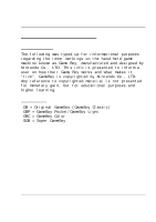
Sources by: Pan of Anthrox, GABY,
Marat Fayzullin,
Pascal Felber, Paul Robson, Martin Korth, kOOPa, Bowser
Contents:
Assembly Language Commands, Timings and Opcodes, and
everything you always wanted to know about GB but were
afraid to ask.
THIS DOCUMENT IS PRINTED ON DIN A5 SIZE PAPER
(148mm x 210mm)!
Note: Game Boy
TM
, Game Boy Pocket
TM
, Super Game Boy
TM
and Game
Boy Color
TM
are registered trademarks of Nintendo CO., LTD.
© 1989 to 1999 by Nintendo CO., LTD.
Version: 1.01 by DP
Game Boy
TM
CPU Manual