Sony STR-K7100 Service Manual - Page 22
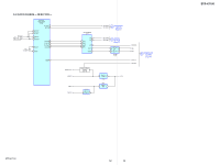
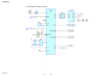
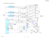
DIGITAL Board, XM Board - parts
 |
View all Sony STR-K7100 manuals
Add to My Manuals
Save this manual to your list of manuals |
Page 22 highlights
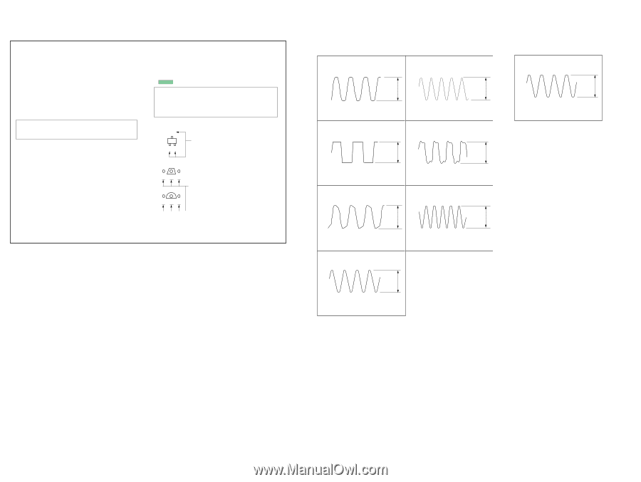
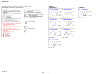
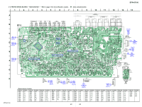
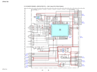
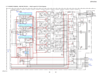
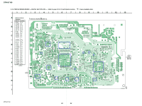
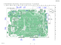
STR-K7100 THIS NOTE IS COMMON FOR PRINTED WIRING BOARDS AND SCHEMATIC DIAGRAMS. (In addition to this, the necessary note is printed in each block.) for schematic diagram: • All capacitors are in µF unless otherwise noted. (p: pF) 50 WV or less are not indicated except for electrolytics and tantalums. • All resistors are in Ω and 1/4 W or less unless otherwise specified. • f : internal component. • 2 : nonflammable resistor. • 5 : fusible resistor. • C : panel designation. Note: The components identified by mark 0 or dotted line with mark 0 are critical for safety. Replace only with part number specified. • A : B+ Line. • B : B- Line. • Voltage and waveforms are dc with respect to ground under no-signal (detuned) conditions. no mark : FM • Voltages are taken with a VOM (Input impedance 10 MΩ). Voltage variations may be noted due to normal production tolerances. • Waveforms are taken with a oscilloscope. Voltage variations may be noted due to normal production tolerances. • Circled numbers refer to waveforms. • Signal path. F : TUNER (FM/AM) L : VIDEO (AUDIO) I : VIDEO J : DVD (DIGITAL) c : CD (ANALOG) for printed wiring boards: • X : parts extracted from the component side. • f : internal component. • : Pattern from the side which enables seeing. Caution: Pattern face side: Parts on the pattern face side seen from the (Side B) pattern face are indicated. Parts face side: Parts on the parts face side seen from the (Side A) parts face are indicated. C Q These are omitted. BE Q BCE Q BCE These are omitted. • Waveforms - DIGITAL Board - 1 IC1301 qd (CKOUT) 5 IC1501 qs (MCLK2) - XM Board - 1 IC102 wh (OSCOUT) 12.288 MHz 1 V/DIV, 50 nsec/DIV 2 IC1301 qf (BCK) 3.8 Vp-p 13.9 MHz 3.2 Vp-p 1 V/DIV, 50 nsec/DIV 6 IC1501 qf (SCKOUT) 45.158 MHz 0.05 V/DIV, 0.2 µsec/DIV 0.07 Vp-p 3.07 MHz 3.6 Vp-p 12.288 MHz 1 V/DIV, 0.2 µs/DIV 3 IC1301 wa (XOUT) 1 V/DIV, 50 nsec/DIV 7 IC1907 tj (X1) 3.5 Vp-p 12.288 MHz 3.1 Vp-p 12.5 MHz 1 V/DIV, 50 nsec/DIV 4 IC1501 9 (MCLK1) 1 V/DIV, 50 nsec/DIV 2.8 Vp-p 13.9 MHz 1 V/DIV, 50 nsec/DIV 1.7 Vp-p STR-K7100 22 22
-
 1
1 -
2
-
3
-
4
-
5
-
6
-
7
-
8
-
9
-
10
-
11
-
12
-
13
-
14
-
15
-
16
-
 17
17 -
 18
18 -
 19
19 -
 20
20 -
 21
21 -
 22
22 -
 23
23 -
 24
24 -
 25
25 -
 26
26 -
 27
27 -
28
-
29
-
30
-
31
-
32
-
33
-
34
-
35
-
36
-
37
-
38
-
39
-
40
-
41
-
42
-
43
-
44
-
45
-
46
-
47
-
48
-
49
-
50
-
51
-
52
-
53
-
54
-
55
-
56
-
57
-
58
-
59
-
60
-
61
-
62
-
63
-
64
-
65
-
66
-
67
-
68
-
69
-
70
-
71
-
72
-
73
-
74
 |
 |