AIWA AM-HX50 Service Manual - Page 20
AIWA AM-HX50 Manual
 |
View all AIWA AM-HX50 manuals
Add to My Manuals
Save this manual to your list of manuals |
Page 20 highlights
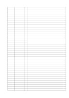
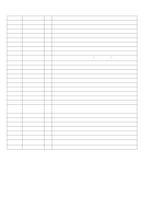
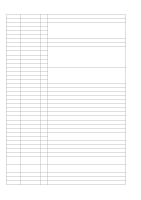
Pin No. 47 48 49 50 51 52 53 54 55 56 57 58 59 60 61-67 68 69 70 71 72 73 74 75 76 77 78 79 80 Pin Name VP MON3 MON2 MON1 MON0 DEFECT PPIT READ SEDIR RESET HOLDER DRAMSW PCK FSEQ NC VSS3 VDD3 MCAS MRAS BUP P-CONT AMUTE RMCDT PWSTB HOLD PLG-I JAPAN TEST I/O Description I VP (CLV servo lock judgement) signal input. I Monitor 3 signal input from LC89641. I Monitor 2 signal input from LC89641. I Monitor 1 signal input from LC89641. I Monitor 0 signal input from LC89641. I DEFECT signal input. I PPIT signal input. O Outputs H during data read. I Direction input of sled movement (inner ™ outer at H, outer ™ inner at L). O LC89641 reset signal output. I Holder OPEN (H)/CLOSE (L) signal input and standby cancel. O Power supply control output of DRAM. (power of DRAM is turned on at L.) I PCK signal input from LC89641. I FSEQ signal input from LC89641. O Not used (L output). - Connected to GND. - Connected to VDD. O CAS signal output to DRAM. O RAS signal output to DRAM. Control selector signal output (controlled by microprocessor at H) over DRAM O microprocessor control/DSP. O System power supply control (power ON at L). O Audio mute signal output (mute ON at H). O Serial data output to LCD remote control. O Standby signal output of headphones driver (standby at L). I HOLD signal input (HOLD ON at L). I Headphones jack insertion detection signal input (insert at L). I Domestic version/foreign version switching input (domestic version at H). I Test mode/main mode switching input (test mode at L). 24


