AIWA AM-HX50 Service Manual - Page 21
IC, LC89641
 |
View all AIWA AM-HX50 manuals
Add to My Manuals
Save this manual to your list of manuals |
Page 21 highlights
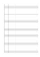
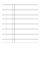
IC, LC89641 Pin No. 1 2 3 4 5 6 7 8 9 10 11 12 13 14 15 16 17 18 19 20 21 22 23 24 25 26 27 28 29 30 31 32 33 34 35 36 37 38 39 40 41 Pin Name SGC AOFFSET FOFFSET TOFFSET TBAL LDREF FG SPPWMF SPPWMR SLPWMF SLPWMR FOPWMF FOPWMR TRPWMF TRPWMR VSS XIN XOUT VDD2 F16M VDD1 ENH LRCO DDATA BCO DDOUT AVDD OUTL OUTR AVSS VDD3 MAD3 MAD2 MAD1 MAD0 MAD9 MAD10 MAD11 MRASB VSS VDD1 I/O Description O AGC control signal output terminal. O ABCD offset control signal output terminal. O Focus offset control signal output terminal. O Tracking offset control signal output terminal. O Tracking balance control signal output terminal. O Laser control signal output terminal. I Speed pulse input terminal. O Spindle PWM output terminal. O O Sled PWM output terminal. O O Focus PWM output terminal. O O Tracking PWM output terminal. O - Ground terminal. I Input terminal for 16.9344 MHz oscillation. O Output terminal for 16.9344 MHz oscillation. - Power terminal. O 16.9344 MHz output terminal. - Internal power supply terminal. O De-emphasis command output terminal. O LR clock output terminal. O Audio extended data output terminal. O Bit clock output terminal. O Digital audio output terminal. - Power supply terminal for 1BIT DAC. O 1BIT DAC L-channel output terminal. O 1BIT DAC R-channel output terminal. - Ground terminal for 1BIT DAC. - Power supply terminal. O O O O Address output terminal to DRAM. O O O ________ O RAS signal output terminal to DRAM. - Ground terminal. - Internal power supply terminal. 25
-
 1
1 -
2
-
3
-
4
-
5
-
6
-
7
-
8
-
9
-
10
-
11
-
12
-
13
-
14
-
15
-
 16
16 -
 17
17 -
 18
18 -
 19
19 -
 20
20 -
 21
21 -
 22
22 -
 23
23 -
 24
24 -
 25
25 -
 26
26 -
27
-
28
-
29
-
30
-
31
-
32
 |
 |
