ASRock AB350M-HDV R3.0 User Manual - Page 57
Write to Read Delay tWTR_L
 |
View all ASRock AB350M-HDV R3.0 manuals
Add to My Manuals
Save this manual to your list of manuals |
Page 57 highlights
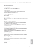
Refresh Cycle Time The Refresh command period. RAS to RAS Delay (tRRD_S) The number of clocks between two rows activated in different banks of the same rank. RAS to RAS Delay (tRRD_L) The number of clocks between two rows activated in different banks of the same rank. Four Activate Window (tFAW) The time window in which four activates are allowed the same rank. Write to Read Delay (tWTR_S) The number of clocks between the last valid write operation and the next read command to the same internal bank. Write to Read Delay (tWTR_L) The number of clocks between the last valid write operation and the next read command to the same internal bank. Write Recovery Time (tWR) The amount of delay that must elapse after the completion of a valid write operation, before an active bank can be precharged. Trcpage (tMAW,MAC) The minimum average time in memory clock cycles within a refresh window from an activate command to another activate command. TrdrdScL The minimum number of cycles from the last clock of virtual CAS of the first readburst operation to the clock in which CAS is asserted for a following read-burst operation in the same chipselect in the same bank group TwrwrScL The minimum number of cycles from the last clock of virtual CAS of a first writeburst operation to the clock in which CAS is asserted for a following write-burst operation in the same bank group. 52 English
-
 1
1 -
2
-
3
-
4
-
5
-
6
-
7
-
8
-
9
-
10
-
11
-
12
-
13
-
14
-
15
-
16
-
17
-
18
-
19
-
20
-
21
-
22
-
23
-
24
-
25
-
26
-
27
-
28
-
29
-
30
-
31
-
32
-
33
-
34
-
35
-
36
-
37
-
38
-
39
-
40
-
41
-
42
-
43
-
44
-
45
-
46
-
47
-
48
-
49
-
50
-
51
-
 52
52 -
 53
53 -
 54
54 -
 55
55 -
 56
56 -
 57
57 -
 58
58 -
 59
59 -
 60
60 -
 61
61 -
 62
62 -
63
-
64
-
65
-
66
-
67
-
68
-
69
-
70
-
71
-
72
-
73
-
74
-
75
-
76
-
77
-
78
-
79
-
80
-
81
-
82
-
83
-
84
-
85
-
86
-
87
 |
 |