ASRock Fatal1ty Z270 Professional Gaming i7 User Manual - Page 75
RAS to RAS Delay tRRD_S
 |
View all ASRock Fatal1ty Z270 Professional Gaming i7 manuals
Add to My Manuals
Save this manual to your list of manuals |
Page 75 highlights
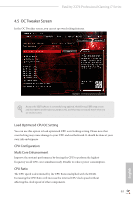
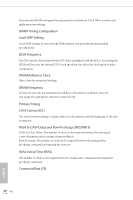
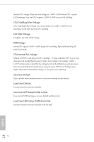
Fatal1ty Z270 Professional Gaming i7 Series The delay between when a memory chip is selected and when the first active command can be issued. Secondary Timing Write Recovery Time (tWR) The amount of delay that must elapse after the completion of a valid write operation, before an active bank can be precharged. Refresh Cycle Time (tRFC) The number of clocks from a Refresh command until the first Activate command to the same rank. RAS to RAS Delay (tRRD_L) The number of clocks between two rows activated in different banks of the same rank. RAS to RAS Delay (tRRD_S) The number of clocks between two rows activated in different banks of the same rank. Write to Read Delay (tWTR_L) The number of clocks between the last valid write operation and the next read command to the same internal bank. Write to Read Delay (tWTR_S) The number of clocks between the last valid write operation and the next read command to the same internal bank. Read to Precharge (tRTP) The number of clocks that are inserted between a read command to a row precharge command to the same rank. Four Activate Window (tFAW) The time window in which four activates are allowed the same rank. CAS Write Latency (tCWL) Configure CAS Write Latency. 67 English
-
 1
1 -
2
-
3
-
4
-
5
-
6
-
7
-
8
-
9
-
10
-
11
-
12
-
13
-
14
-
15
-
16
-
17
-
18
-
19
-
20
-
21
-
22
-
23
-
24
-
25
-
26
-
27
-
28
-
29
-
30
-
31
-
32
-
33
-
34
-
35
-
36
-
37
-
38
-
39
-
40
-
41
-
42
-
43
-
44
-
45
-
46
-
47
-
48
-
49
-
50
-
51
-
52
-
53
-
54
-
55
-
56
-
57
-
58
-
59
-
60
-
61
-
62
-
63
-
64
-
65
-
66
-
67
-
68
-
69
-
 70
70 -
 71
71 -
 72
72 -
 73
73 -
 74
74 -
 75
75 -
 76
76 -
 77
77 -
 78
78 -
 79
79 -
 80
80 -
81
-
82
-
83
-
84
-
85
-
86
-
87
-
88
-
89
-
90
-
91
-
92
-
93
-
94
-
95
-
96
-
97
-
98
-
99
-
100
-
101
-
102
-
103
-
104
-
105
-
106
 |
 |