ASRock K7VT2 User Manual - Page 11
Jumpers Setup, 8 Connectors
 |
View all ASRock K7VT2 manuals
Add to My Manuals
Save this manual to your list of manuals |
Page 11 highlights
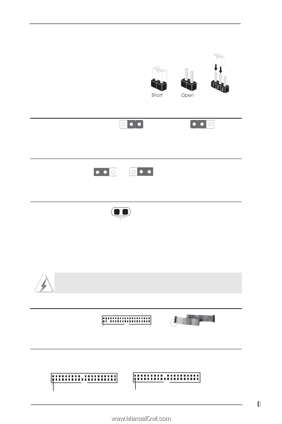
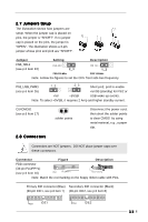
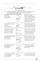
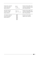
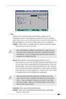
2.7 Jumpers Setup The illustration shows how jumpers are setup. When the jumper cap is placed on pins, the jumper is "SHORT". If no jumper cap is placed on the pins, the jumper is "OPEN". The illustration shows a 3-pin jumper whose pin1 and pin2 are "SHORT". Jumper Setting Description FSB_SEL1 (see p.6 item 23) FSB_SEL1 2_3 FSB_SEL1 1_2 FSB 100 MHz FSB 133 MHz Note: Follow the figures to set the CPU front side bus frequency. PS2_USB_PWR1 1_2 2_3 Short pin2, pin3 to enable (see p.6 item 26) +5VSB (standby) for PS/2 or +5V +5VSB USB wake up events. Note: To select +5VSB, it requires 2 Amp and higher standby current. CLRCMOS1 (see p.6 item 17) solder points 2.8 Connectors Disconnect the power cord, then short the solder points to clear CMOS by using metal material, e.g., a paper clip. Connectors are NOT jumpers. DO NOT place jumper caps over these connectors. Connector Figure Description FDD connector (33-pin FLOPPY1) (see p.6 item 10) Pin1 FLOPPY1 Red marking Note: Match the red marking on the floppy ribbon cable with Pin1. Primary IDE connector (Blue) Secondary IDE connector (Black) (39-pin IDE1, see p.6 item 7) (39-pin IDE2, see p.6 item 8) PIN1 IDE1 PIN1 IDE2 11
-
 1
1 -
2
-
3
-
4
-
5
-
 6
6 -
 7
7 -
 8
8 -
 9
9 -
 10
10 -
 11
11 -
 12
12 -
 13
13 -
 14
14 -
 15
15 -
 16
16 -
17
-
18
-
19
-
20
-
21
-
22
-
23
-
24
 |
 |