ASRock PE PRO-HT User Manual - Page 11
Connectors
 |
View all ASRock PE PRO-HT manuals
Add to My Manuals
Save this manual to your list of manuals |
Page 11 highlights
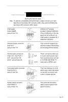
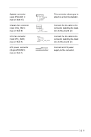
Jumper PS2_USB_PWR1 (see p.6 item 22) Setting 1_2 +5V 2_3 +5VSB Description Short pin2, pin3 to enable +5VSB (standby) for PS/2 or USB wake up events. Note: To select +5VSB, it requires 2 Amp and higher standby current provided by power supply. Clear CMOS CLRCMOS1 (see p.6 item 17) solder points Description To clear and reset the system parameters to default setup, please turn off the computer and unplug the power cord, then short the solder points for more than 3 seconds by using metal material, e.g., a paper clip. Note:These solder points allow you to clear the data in CMOS. The data in CMOS includes system setup information such as system password, date, time, and system setup parameters. 2.8 Connectors Connectors are NOT jumpers. DO NOT place jumper caps over these connectors. Connector Figure Description FDD connector (33-pin FLOPPY1) (see p.6 item 10) Pin1 FLOPPY1 Red marking Note: Match the red marking on the floppy ribbon cable with Pin1. Primary IDE connector (Blue) (39-pin IDE1) (see p.6 item 7) Secondary IDE connector (Black) (39-pin IDE2) (see p.6 item 8) PIN1 IDE1 PIN1 IDE2 11
-
 1
1 -
2
-
3
-
4
-
5
-
 6
6 -
 7
7 -
 8
8 -
 9
9 -
 10
10 -
 11
11 -
 12
12 -
 13
13 -
 14
14 -
 15
15 -
 16
16 -
17
-
18
-
19
-
20
-
21
-
22
-
23
-
24
-
25
 |
 |
