Asus P I-P65UP5 C-PKND User Manual - Page 10
Iii. Installation
 |
View all Asus P I-P65UP5 C-PKND manuals
Add to My Manuals
Save this manual to your list of manuals |
Page 10 highlights
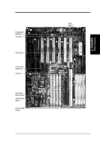
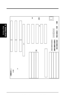
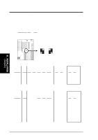
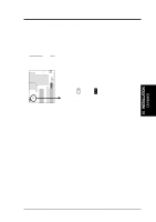
III. INSTALLATION Map of the Baseboard JP4 Boot Block Progam Disable/Enable Universal Serial Bus (Reserved for future) JP1 Keyboard Serial Ports Parallel Port COM 1 COM 2 Board Power Input P9 P8 Floppy Drives Secondary IDE Primary IDE SIMM Socket 7 (Bank 3) SIMM Socket 5 (Bank 2) SIMM Socket 3 (Bank 1) SIMM Socket 1 (Bank 0) CPU Card Slot PCI Slot 1 Multi-I/O Enable/Disable PCI Slot 2 PCI Slot 3 PCI Slot 4 BUS Freq. CPU Card Slot SIMM Socket 8 (Bank 3) JP2 JP3 SIMM Socket 6 (Bank 2) SIMM Socket 4 (Bank 1) SIMM Socket 2 (Bank 0) PCI Slot 5 / MediaBus 2.0 ISA Slot 1 ISA Slot 2 ISA Slot 3 III. INSTALLATION (Map of Board) IDE LED JP7 RTC RAM Operation/Clear Infrared Con Case Connector 4 ASUS P/I-P65UP5 User's Manual
-
 1
1 -
2
-
3
-
4
-
 5
5 -
 6
6 -
 7
7 -
 8
8 -
 9
9 -
 10
10 -
 11
11 -
 12
12 -
 13
13 -
 14
14 -
 15
15 -
16
-
17
-
18
-
19
-
20
-
21
-
22
-
23
-
24
-
25
-
26
-
27
-
28
-
29
-
30
-
31
-
32
 |
 |

4
ASUS P/I-P65UP5 User's Manual
III. INSTALLATION
Map of the Baseboard
SIMM Socket 1 (Bank 0)
SIMM Socket 3 (Bank 1)
SIMM Socket 5 (Bank 2)
SIMM Socket 7 (Bank 3)
SIMM Socket 2 (Bank 0)
SIMM Socket 4 (Bank 1)
SIMM Socket 6 (Bank 2)
SIMM Socket 8 (Bank 3)
ISA Slot 3
ISA Slot 2
ISA Slot 1
PCI Slot 5 / MediaBus 2.0
PCI Slot 3
PCI Slot 2
PCI Slot 1
PCI Slot 4
CPU Card Slot
Keyboard
COM 1
COM 2
Case Connector
Infrared Con
IDE LED
JP4
JP1
CPU Card Slot
Floppy Drives
Secondary IDE
Primary IDE
Parallel Port
Board Power Input
P9
P8
Boot Block Progam
Disable/Enable
Universal Serial Bus
(Reserved for future)
JP7
RTC RAM
Operation/Clear
Multi-I/O Enable/Disable
JP2
JP3
BUS Freq.
Serial Ports
(Map of Board)
III.
INSTALLATION