Biostar M7VIG M7VIG user's manual - Page 55
CPU & PCI Bus Control, Memory Hole, System BIOS Cacheable, PCI2 Master 0 WS Write
 |
View all Biostar M7VIG manuals
Add to My Manuals
Save this manual to your list of manuals |
Page 55 highlights
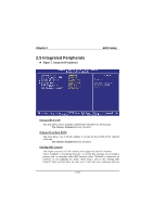
Chapter 2 BIOS Setup CPU & PCI Bus Control If you highlight the literal "Press Enter" next to the "CPU & PCI Bus Control" label and then press the enter key, it will take you a submenu with the following options: PCI1 Master 0 WS Write When enabled, writes to the PCI bus are executed with zero-wait states. The Choices: Enabled (default), Disabled. PCI2 Master 0 WS Write When enabled, writes to the AGP bus are executed with zero-wait states. The Choices: Enabled (default), Disabled. PCI1 Post Write When Enabled, CPU writes are allowed to post on the PCI bus. The Choices: Enabled (default), Disabled. PCI2 Post Write When Enabled, CPU writes are allowed to post on the AGP bus. The Choices: Enabled (default), Disabled. PCI Delay Transaction The chipset has an embedded 32-bit posted write buffer to support delay transactions cycles. Select Enabled to support compliance with PCI specification. The Choices: Enabled (default), Disabled. Memory Hole When enabled, you can reserve an area of system memory for ISA adapter ROM. When this area is reserved, it cannot be cached. Refer to the user documentation of the peripheral you are installing for more information. The Choices: Disabled (default), 15M - 16M. System BIOS Cacheable Selecting the "Enabled" option allows caching of the system BIOS ROM at F0000h-FFFFFh, which can improve system performance. However, any programs writing to this area of memory will cause conflicts and result in system errors. The Choices: Enabled, Disabled (default). 2-16
-
 1
1 -
2
-
3
-
4
-
5
-
6
-
7
-
8
-
9
-
10
-
11
-
12
-
13
-
14
-
15
-
16
-
17
-
18
-
19
-
20
-
21
-
22
-
23
-
24
-
25
-
26
-
27
-
28
-
29
-
30
-
31
-
32
-
33
-
34
-
35
-
36
-
37
-
38
-
39
-
40
-
41
-
42
-
43
-
44
-
45
-
46
-
47
-
48
-
49
-
 50
50 -
 51
51 -
 52
52 -
 53
53 -
 54
54 -
 55
55 -
 56
56 -
 57
57 -
 58
58 -
 59
59 -
 60
60 -
61
-
62
-
63
-
64
-
65
-
66
-
67
-
68
-
69
-
70
-
71
-
72
-
73
-
74
-
75
-
76
-
77
-
78
-
79
 |
 |