Gigabyte GA-J1800N-D2P User Manual - Page 5
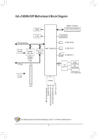
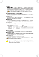
GA-J1800N-D2P Motherboard Block Diagram
 |
View all Gigabyte GA-J1800N-D2P manuals
Add to My Manuals
Save this manual to your list of manuals |
Page 5 highlights
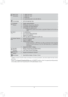
GA-J1800N-D2P Motherboard Block Diagram HDMI DDR3L 1333 MHz Dual Channel Memory D-Sub Dual BIOS PCI Express Bus PCIe CLK (100 MHz) x1 Realtek® GbE LAN RJ45 LAN PCI Bus x1 PCIe to PCI Bridge Intel® J1800 SoC 2 SATA 3Gb/s 2 USB 3.0/2.0 4 USB 2.0/1.1 LPC Bus iTE® Super I/O COM LPT PCI CLK (33 MHz) 1 PCI CODEC PS/2 KB/Mouse MIC (Center/Subwoofer Speaker Out) Line Out (Front Speaker Out) Line In (Rear Speaker Out) S/PDIF Out For detailed product information/limitation(s), refer to "1-2 Product Specifications." - 5 -
-
 1
1 -
 2
2 -
 3
3 -
 4
4 -
 5
5 -
 6
6 -
 7
7 -
 8
8 -
 9
9 -
 10
10 -
 11
11 -
12
-
13
-
14
-
15
-
16
-
17
-
18
-
19
-
20
-
21
-
22
-
23
-
24
-
25
-
26
-
27
-
28
-
29
-
30
-
31
-
32
 |
 |

- 5 -
GA-J1800N-D2P Motherboard Block Diagram
PS/2 KB/Mouse
Intel
®
J1800 SoC
Dual BIOS
COM
LPT
LPC
Bus
DDR3L 1333 MHz
LAN
RJ45
PCI Express Bus
PCIe CLK
(100 MHz)
Realtek
®
GbE LAN
2 SATA 3Gb/s
2 USB 3.0/2.0
4 USB 2.0/1.1
D-Sub
HDMI
Dual Channel Memory
x1
iTE
®
Super I/O
For detailed product information/limitation(s), refer to "1-2 Product Specifications."
Line Out (Front Speaker Out)
MIC (Center/Subwoofer
Speaker Out)
Line In (Rear Speaker Out)
CODEC
PCI Bus
x1
PCIe to PCI
Bridge
PCI CLK
(33 MHz)
1 PCI
S/PDIF Out