Gigabyte GA-N3160TN User Manual - Page 15
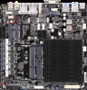
BL_SW Back Light Switch, LVDS LVDS Header, LCD_VCC LVDS Drive Voltage Jumper
 |
View all Gigabyte GA-N3160TN manuals
Add to My Manuals
Save this manual to your list of manuals |
Page 15 highlights
13) LVDS (LVDS Header) LVDS stands for Low-voltage differential signaling, which uses high-speed analog circuit techniques to provide multigigabit data transfers on copper interconnects and is a generic interface standard for highspeed data transmission. Pin No. Definition Pin No. Definition Pin No. Definition 2 1 1 LCD_VCC 2 LCD_VCC 15 -RXO3_C 16 +RXO3_C 29 CABLE_DET(Note) 30 -RXE3_C 3 VCC3 17 GND 31 +RXE3_C 4 NC 18 -RXECLKO_C 32 GND 5 NC 19 +RXECLKO_C 33 -RXECLKE_C 6 -RXO0_C 20 GND 34 +RXECLKE_C 7 +RXO0_C 21 -RXE0_C 35 GND 40 39 8 GND 9 -RXO1_C 22 +RXE0_C 23 GND 36 SC_BKLT_EN 37 SC_BKLT_CTL 10 +RXO1_C 24 -RXE1_C 38 FPD_PWR 11 GND 25 +RXE1_C 39 FPD_PWR 12 -RXO2_C 26 GND 40 FPD_PWR 13 +RXO2_C 27 -RXE2_C 14 GND 28 +RXE2_C (Note) Connects to the ground pin of the LVDS. 14) BL_SW (Back Light Switch) The Back Light switch provides the function for screen back light adjustment. Pin No. Definition 1 1 BL_DOWN 2 BL_UP 15) LCD_VCC (LVDS Drive Voltage Jumper) This jumper can be used to provide different screen voltage settings. 1-2 Close: Set to 3V. (Default setting) 1 1 2-3 Close: Set to 5V. 16) MON_SW (Flat Panel Display Switch Header) This header allows you to connect an on/off switch for the display. Pin No. Definition 1 1 Mon_SW 2 GND - 15 -
-
 1
1 -
2
-
3
-
4
-
5
-
6
-
7
-
8
-
9
-
 10
10 -
 11
11 -
 12
12 -
 13
13 -
 14
14 -
 15
15 -
 16
16 -
 17
17 -
 18
18 -
 19
19 -
 20
20 -
21
-
22
-
23
-
24
-
25
-
26
-
27
-
28
-
29
-
30
-
31
-
32
-
33
-
34
 |
 |
