HP DL740 hot plug RAID memory technology for fault tolerance and scalability - Page 6
basic operation, In a memory read transaction
 |
UPC - 808736765770
View all HP DL740 manuals
Add to My Manuals
Save this manual to your list of manuals |
Page 6 highlights
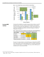
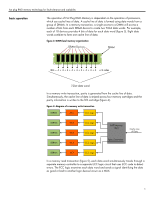
hot plug RAID memory technology for fault tolerance and scalability basic operation The operation of Hot Plug RAID Memory is dependant on the operation of processors, which use cache lines of data. A cache line of data is formed using data words from a group of DIMMs. In a memory transaction, a single access to a DIMM will access a number of bits from each DRAM device to create two 72-bit data words. For example, each of 18 devices provides 4 bits of data for each data word (figure 3). Eight data words combine to form one cache line of data. figure 3: DIMM-level memory organization DRAM Devices DIMM Bits = 4 + 4 + 4 + 4 + 4 + 4 + 4 + 4 + 4 x 2 sides 72-bit data word In a memory write transaction, parity is generated from the cache line of data. Simultaneously, the cache line of data is striped across four memory cartridges and the parity information is written to the fifth cartridge (figure 4). figure 4: diagram of a memory write transaction SDRAM MC1 ECC Logic SDRAM SDRAM SDRAM MC2 MC3 MC4 ECC Logic ECC Logic ECC Logic RAID Memory Logic Cache Line of Data Parity Generation SDRAM MCP ECC Logic In a memory read transaction (figure 5), each data word simultaneously travels through a separate memory controller to a separate ECC logic circuit that uses ECC code to detect errors. The ECC logic examines each data word and sends a signal identifying the data as good or bad to another logic device known as a MUX. 6
-
 1
1 -
 2
2 -
 3
3 -
 4
4 -
 5
5 -
 6
6 -
 7
7 -
 8
8 -
 9
9
 |
 |
