HP DL740 hot plug RAID memory technology for fault tolerance and scalability - Page 7
If the signal from the ECC logic to the MUX indicates the data is good, the MUX sends, MUX
 |
UPC - 808736765770
View all HP DL740 manuals
Add to My Manuals
Save this manual to your list of manuals |
Page 7 highlights
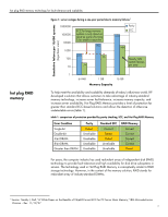
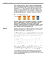
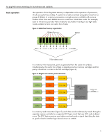
hot plug RAID memory technology for fault tolerance and scalability figure 5: diagram of a memory read transaction for one of the four data paths SDRAM MC1 ECC Logic MUX Good Data SDRAM SDRAM SDRAM MC2 MC3 MC4 ECC Logic ECC Logic ECC Logic RAID Memory Logic Parity Compare Miscompare = NMI, if ECC did not report it SDRAM MCP ECC Logic During every read transaction, the ECC logic also passes data to a RAID memory logic circuit where a RAID algorithm simultaneously regenerates each data word using the data words from the other three memory controllers and the parity controller. For example, as shown in figure 5, the RAID memory logic uses the data words from memory controllers 2, 3, 4, and P to regenerate the data word for memory controller 1 (MC1). Each regenerated data word from the RAID memory logic is then passed to a separate MUX (figure 6). figure 6: RAID memory architecture SDRAM SDRAM MC1 ECC Logic MC2 ECC Logic SDRAM MC3 ECC Logic SDRAM MC4 ECC Logic RAID Memory Logic MUX 1 PC1 MUX 2 PC2 MUX 3 PC3 MUX 4 PC4 SDRAM MCP ECC Logic If the signal from the ECC logic to the MUX indicates the data is good, the MUX sends the original data to the processor. If the signal from the ECC logic to the MUX indicates the data has an error, the MUX sends the regenerated data from the RAID memory logic. At this point, the error detected by the ECC logic has been eliminated and only good data has been transmitted. 7
-
 1
1 -
 2
2 -
 3
3 -
 4
4 -
 5
5 -
 6
6 -
 7
7 -
 8
8 -
 9
9
 |
 |
