HP Vectra VL800 hp vectra vl800, technical reference manual - desktop and mini - Page 55
Main Memory Controller
 |
View all HP Vectra VL800 manuals
Add to My Manuals
Save this manual to your list of manuals |
Page 55 highlights
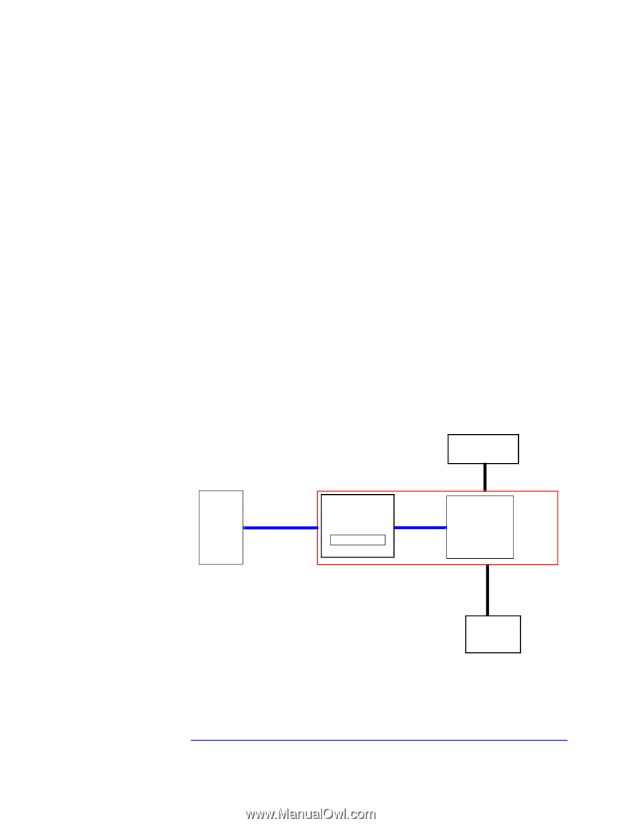
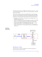
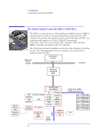
3 System Board Memory Controller Hub (82850) AGP PCI Bus Implementation The AGP bus is based upon a 66 MHz, 32-bit PCI bus architecture, to which several signal groups have been added to provide AGP-specific control and transfer mechanisms. AGP specific transactions always use pipelining. This control mechanism increases the bus efficiency for data transfer. Sideband Addressing (SBA) may also be used by AGP transaction requests which further increases the bus efficiency for data transfer. The supported modes are detailed below: • FRAME-based AGP. Only the PCI semantics are: 66 MHz, 32-bit, 1.5 V, 266 MB/s peak transfer rate. • AGP 1X with pipelining, sideband addressing can be added: uses 66 MHz, 32-bit, 1.5 V, increased bus efficiency, 266 MB/s peak transfer rate. • AGP 2X with pipelining, sideband addressing can be added: 66 MHz double clocked, 32-bit, 1.5 V, 533 MB/s peak transfer rate. • AGP 4X with pipelining, sideband addressing can be added: 133 MHz double clocked, 32-bit, 1.5 V, increased bus efficiency, 1066 MB/s peak transfer rate Pentium 4 Processor 1.5V AGP Connector AGP 4x Bus (133 MHz) GX-Device 1 AGP Port Interface PCI-to-PCI Device 0 I850 Memory Controller Hub (MCH) Hub Link 8-bit I/O Controller Hub (ICH2) Main Memory Controller The main memory controller is integrated in the MCH supporting two primary rambus channels (A and B). 55
-
 1
1 -
2
-
3
-
4
-
5
-
6
-
7
-
8
-
9
-
10
-
11
-
12
-
13
-
14
-
15
-
16
-
17
-
18
-
19
-
20
-
21
-
22
-
23
-
24
-
25
-
26
-
27
-
28
-
29
-
30
-
31
-
32
-
33
-
34
-
35
-
36
-
37
-
38
-
39
-
40
-
41
-
42
-
43
-
44
-
45
-
46
-
47
-
48
-
49
-
 50
50 -
 51
51 -
 52
52 -
 53
53 -
 54
54 -
 55
55 -
 56
56 -
 57
57 -
 58
58 -
 59
59 -
 60
60 -
61
-
62
-
63
-
64
-
65
-
66
-
67
-
68
-
69
-
70
-
71
-
72
-
73
-
74
-
75
-
76
-
77
-
78
-
79
-
80
-
81
-
82
-
83
-
84
-
85
-
86
-
87
-
88
-
89
-
90
-
91
-
92
-
93
-
94
-
95
-
96
-
97
-
98
-
99
-
100
-
101
-
102
-
103
-
104
-
105
-
106
-
107
-
108
-
109
-
110
-
111
-
112
-
113
-
114
-
115
-
116
-
117
-
118
-
119
-
120
-
121
-
122
-
123
-
124
-
125
-
126
-
127
-
128
-
129
-
130
-
131
-
132
-
133
-
134
-
135
-
136
-
137
-
138
-
139
-
140
-
141
-
142
-
143
-
144
-
145
-
146
-
147
 |
 |